AAT3125
USB OTG 5V Charge Pump
3125.2005.12.1.4
1
General Description
The AAT3125 USB On-the-Go (OTG) charge pump
is a member of AnalogicTech's Total Power
Management ICTM (TPMICTM) product family. The
device integrates a high efficiency 1.5X fractional
100mA regulated charge pump for supplying V
BUS
with the additional functions required for OTG
devices (formerly known as dual role devices).
Four voltage detectors monitor V
BUS
, and a current
source dedicated for V
BUS
pulsing is provided for
compliance with Session Request Protocol (SRP)
as defined by the USB OTG Supplement.
The charge pump section uses a high efficiency
fractional topology, with a high frequency 750kHz
switching speed which enables the use of small
capacitors (less than 3.3µF). The AAT3125 fea-
tures extremely low quiescent current to extend
battery run time. Additionally, the device integrates
protection features such as under-voltage lockout,
and output short circuit and thermal protection.
The AAT3125 is available in a Pb-free, surface
mount QFN44-16 package and is rated over the
-40∞C to +85∞C temperature range.
Features
∑
V
IN
Range: 2.7V to 5.5V
∑
Regulated Fractional Charge Pump
∑
100mA Output Current
∑
Reverse Load Protection
∑
Power Good Flag
∑
SRP Detection Flag
∑
SRP Ready Flag
∑
Output Short-Circuit and Thermal Protection
∑
Under-Voltage Protection
∑
Less than 1µA Consumed While Disabled
∑
Designed to Allow Operation with Output
Capacitance as Low as 3.3µF
∑
16-pin QFN44 Package
∑
-40∞C to +85∞C Temperature Range
Applications
∑
Cell Phones
∑
Hand-Held Computers
∑
PDAs
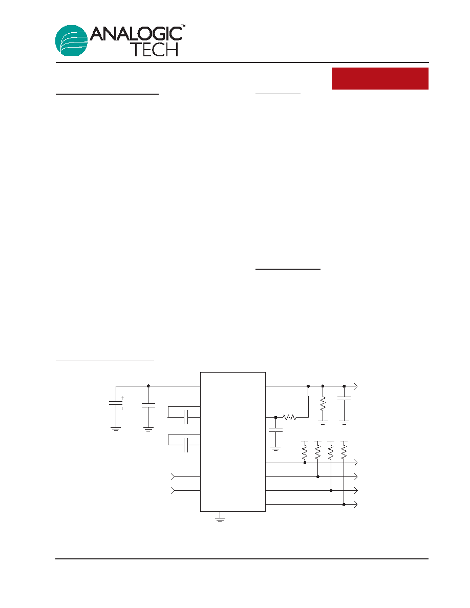
Typical Application
IN
POK1
GND
SR
OUT
C
OUT
C
IN
1
µ
F
1
µ
F
1
µ
F
1
µ
F
3.3
µ
F to 6.5
µ
F
SR
POK2
SESDET
SRRDY
EN
EN
R1
R2
R3
R4
POK1
VBUS
POK2
SESDET
SRRDY
AAT3125
1 Cell
Li-Ion
C1
C2
C1+
C1-
C2+
C2-
80k
C
CP
OUTCP
R
CS
0.2
ChargePump
TM

Pin Descriptions
Pin Configuration
QFN44-16
(Top View)
1
2
3
4
12
11
10
9
5
6
7
8
16
15
14
13
POK1
POK2
SESDET
SRRDY
OUT
C1+
C1-
N/C
OUTCP
C2+
C2-
GND
N/C
VIN
SR
EN
Pin #
Symbol
Function
1 POK1 Power OK 1. Open drain output with 4.0V voltage detector. When the OUT pin rises above the
detected voltage (4.0V), POK1 will transition from low to high state. Similarly, when the output
falls below 4.0V, POK1 will transition from high to low. A 10k
pull-up resistor is recommended.
2 POK2 Power OK 2. Open drain output with 4.4V voltage detector. When the OUT pin rises above the
detected voltage (4.4V), POK2 will transition from low to high state. Similarly, when the output
falls below 4.4V, POK2 will transition from high to low. A 10k
pull-up resistor is recommended.
3 SESDET
Session detect. Open drain output with 2.0V voltage detector. When the OUT pin rises above the
detected voltage (2.0V), it will transition from low to high state. Similarly, when the output falls
below 2.0V, SESDET will transition from high to low. A 10k
pull-up resistor is recommended.
4
SRRDY
Session request ready. Open drain output with 0.6V voltage detector. When the OUT pin rises
above the detected voltage (0.6V), it will transition from low to high state. Similarly, when the
output falls below 0.6V, SRRDY will transition from high to low. A 10k
pull-up resistor is rec-
ommended.
5
OUT
Power output to VBUS.
6
C1+
Flying capacitor 1 positive terminal.
7
C1-
Flying capacitor 1 negative terminal.
8, 13
N/C
No connect.
9
OUTCP
Charge pump output. Requires 1µF bypass capacitor to ground.
10
C2+
Flying capacitor 2 positive terminal.
11
C2-
Flying capacitor 2 negative terminal.
12 GND Ground.
14
VIN
Input power supply. Requires 1µF bypass capacitor to ground.
15
SR
Session request input control pin. Should not be left floating. Must connect to high or low. For
more details, see Table 1.
16
EN
Enable input control pin. When in the low state, the AAT3125 is powered down and consumes
a small amount of power. When connected high, it is in normal operation. This pin should not
be left floating. For more details, see Table 1.
EP
Exposed paddle (bottom); connect to GND directly beneath package.
AAT3125
USB OTG 5V Charge Pump
2
3125.2005.12.1.4

AAT3125
USB OTG 5V Charge Pump
3125.2005.12.1.4
3
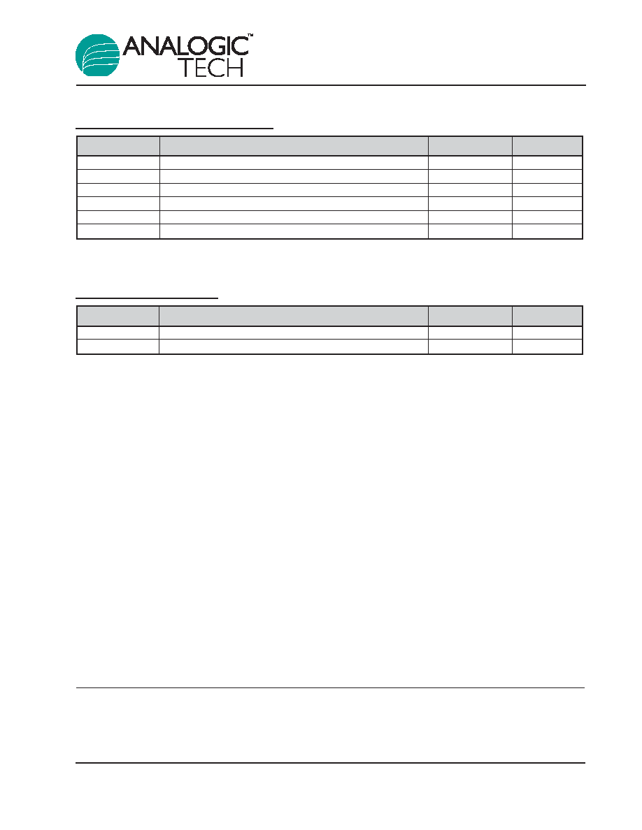
Absolute Maximum Ratings
1
Thermal Information
Symbol
Description
Value
Units
JA
Maximum Thermal Resistance
4
50
∞C/W
P
D
Maximum Power Dissipation (T
A
= 25∞C)
5
2.0
W
Symbol
Description
Value
Units
V
IN
, V
OUT
Any Pin to GND
-0.3 to 6
V
t
SC
OUT Short-Circuit Duration
Indefinite
s
I
OUT
2
Output Current
150
mA
T
J
Operating Temperature Range
-40 to 85
∞C
T
S
Storage Temperature Range
-65 to 150
∞C
V
ESD
ESD Rating
3
- HBM
2000
V
1. Stresses above those listed in Absolute Maximum Ratings may cause permanent damage to the device. Functional operation at condi-
tions other than the operating conditions specified is not implied. Only one Absolute Maximum Rating should be applied at any one time.
2. Based on long-term current density limitation.
3. Human body model is a 100pF capacitor discharged through a 1.5k
resistor into each pin.
4. Mounted on an FR4 board.
5. Derate 20mW/∞C above 25∞C.

AAT3125
USB OTG 5V Charge Pump
4
3125.2005.12.1.4
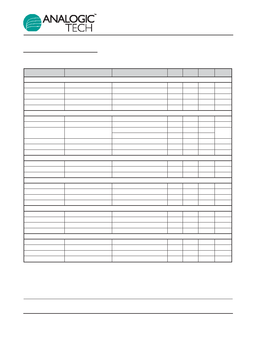
Electrical Characteristics
1
V
IN
= 3.5V; C
IN
= C
OUT
= C
1
= C
2
= 1.0µF; T
A
= -40∞C to +85∞C.
Unless otherwise noted, typical values are T
A
= 25∞C.
Symbol
Description
Conditions
Min
Typ
Max
Units
Input Power Supply
V
IN
Operating Range
2.9
5.5
V
I
cc3
Operating Current SRP
EN = 1, SR = 1, OUT = IN
60
110
µA
I
cc2
Operating Current CP
EN = 1, SR = 0
1
3
mA
I
cc1
Shutdown Current 1
EN = 0, SR = 1
1
2
µA
I
cc0
Shutdown Current 0
EN = 0, SR = 0
1
µA
Output Power Supply
V
OUT
Output Regulation
I
OUT
= 0
4.6
5.25
V
I
CCOUT
Operating Current
EN = 0
7
12
µA
I
OUT
Output Current
3.2
V
IN
5.5V, V
OUT
> 4.4V
50
65
mA
3.35
V
IN
5.5V, V
OUT
> 4.4V
100
V
CS
Current Sense Trip Level
VCS = I
OUT
x R
CS
40
60
90
mV
R
OFF
Pull-Down Resistance
EN = 0, SR = 1
700
1000
1500
I
SR
SR Current Pulse
OUT < (IN-1.0v)
5
10
20
mA
Charge Pump
Efficiency
V
IN
= 3.75V, I
OUT
= 50mA
90
%
T
SS
Soft-Start Time
OUT < 0.1 to OUT > 4.4
100
µs
F
CLK
Clock Frequency
750
kHz
EN, SR
V
IL
Input Threshold Low
0.4
V
V
IH
Input Threshold High
1.4
V
I
EN(SINK)
EN Input Current
V
IN
= V
EN
= 5.5V
-1
1
µA
I
SR(SINK)
SR Input Current
V
IN
= V
SR
= 5.5V
-1
1
µA
POK1
V
POK1
POK Trip Threshold
V
OUT
Rising
3.8
4.0
4.2
V
V
POK1(HYS)
POK Hysteresis
50
mV
V
POK1(OL)
POK Output Voltage
I
SINK
= 1mA
0.3
V
I
POK1
POK Leakage Current
V
POK
= 5.5, 25∞C
100
nA
POK2
V
POK2
POK Trip Threshold
V
OUT
Rising
4.18
4.4
4.62
V
V
POK2(HYS)
POK Hysteresis
50
mV
V
POK2(OL)
POK Output Voltage
I
SINK
= 1mA
0.3
V
I
POK2
POK Leakage Current
V
POK
= 5.5, 25∞C
100
nA
1. The AAT3125 is guaranteed to meet performance specifications over the -40∞C to +85∞C operating temperature range and is assured
by design, characterization, and correlation with statistical process controls.

Electrical Characteristics
1
V
IN
= 3.5V; C
IN
= C
OUT
= C
1
= C
2
= 1.0µF; T
A
= -40∞C to +85∞C.
Unless otherwise noted, typical values are T
A
= 25∞C.
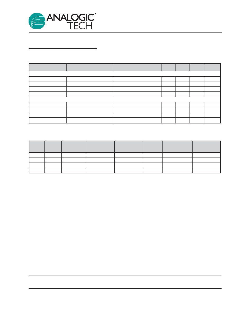
Table 1: Operational States.
Charge Current
Discharge
EN
SR
Pump
Source
SRRDY
POK
SESDET
Resistor
1
0
ON
OFF
ON
ON
ON
OFF
1
1
OFF
ON
ON
ON
ON
OFF
0
0
OFF
OFF
OFF
OFF
ON
OFF
0
1
OFF
OFF
OFF
OFF
ON
ON
Symbol
Description
Conditions
Min
Typ
Max
Units
SESDET
V
SD
SD Trip Threshold
V
OUT
Rising
1.9
2.0
2.1
V
V
SD(HYS)
SD Hysteresis
50
mV
V
SD(OL)
SD Output Voltage
I
SINK
= 1mA
0.3
V
I
SD
SD Leakage Current
V
SD
= 5.5, 25∞C
100
nA
SRRDY
V
SRRDY
SRRDY Trip Threshold
V
OUT
Rising
0.4
0.6
0.8
V
V
SRRDY(HYS)
SRRDY Hysteresis
20
mV
V
SRRDY(OL)
SRRDY Output Voltage
I
SINK
= 1mA
0.3
V
I
SRRDY
SRRDY Leakage Current
V
SRRDY
= 5.5, 25∞C
100
nA
AAT3125
USB OTG 5V Charge Pump
3125.2005.12.1.4
5
1. The AAT3125 is guaranteed to meet performance specifications over the -40∞C to +85∞C operating temperature range and is assured
by design, characterization, and correlation with statistical process controls.
