AAT3129
High Efficiency 1X/1.5X/2X Charge Pump
for RGB Color LED Applications
3129.2005.11.1.3
1
ChargePump
TM
General Description
The AAT3129 is a high efficiency charge pump
DC/DC converter with tri-mode load switch (1X)
fractional (1.5X) and doubling (2X) conversion for
color LED applications. A single current source out-
put provides a regulated current to drive R, G, and
B LEDs via three internal switches. With a simple
single wire serial bus, the RGB module can be eas-
ily controlled to display 4096 colors.
AnalogicTech's Advanced Simple Serial ControlTM
(AS
2
CwireTM) serial digital input is used to enable,
disable, and set the duty cycle of each internal
MOSFET switch. Low external parts count (two
1µF flying capacitors and two small bypass capac-
itors at V
IN
and OUT) makes the AAT3129 ideally
suited for small battery-powered applications.
The AAT3129 has a thermal management system
to protect the device in the event of a short-circuit
condition on any of the output pins. Built-in soft-
start circuitry prevents excessive inrush current
during start-up. High switching frequency enables
the use of small external capacitors. A low current
shutdown feature disconnects the load from V
IN
and reduces quiescent current to less than 1µA.
The AAT3129 is available in a Pb-free, 12-pin
TSOPJW package.
Features
∑
V
IN
Range: 2.7V to 5.5V
∑
Common Anode RGB LED Control
∑
4096 Color with Single Wire Digital Control
∑
40mA to 180mA Fixed Current Source
∑
AS
2
Cwire Digital Brightness Control
∑
Low Noise Constant Frequency Operation
∑
Small Application Circuit
∑
Regulated Output Current
∑
No Inductors
∑
1MHz Switching Frequency
∑
I
Q
<1µA in Shutdown
∑
12-Pin TSOPJW Package
Applications
∑
Fashion RGBs
∑
Mobile Handsets
∑
MP3 Players
∑
PDAs
∑
Portable Devices
∑
RGB Color LEDs
∑
RGB Photo Flash
∑
Smart Phones
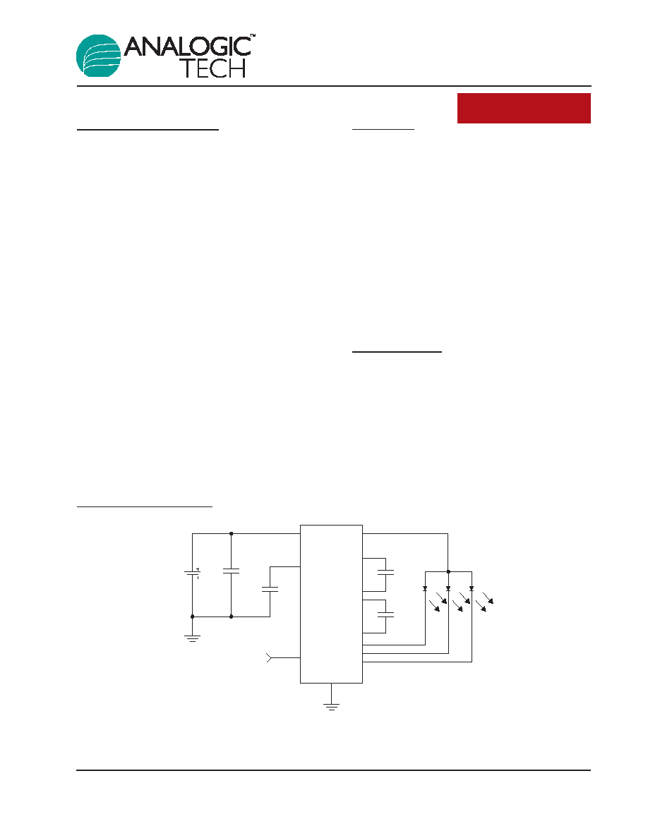
Typical Application
C
IN
1
µF
V
BAT
C
CP
1
µF
C1
1
µF
C2
1
µF
VIN
CP
C1+
C1-
C2+
C2-
DR
DG
DB
EN/SET
EN/SET
GND
AAT3129
G
R
B
ISRC
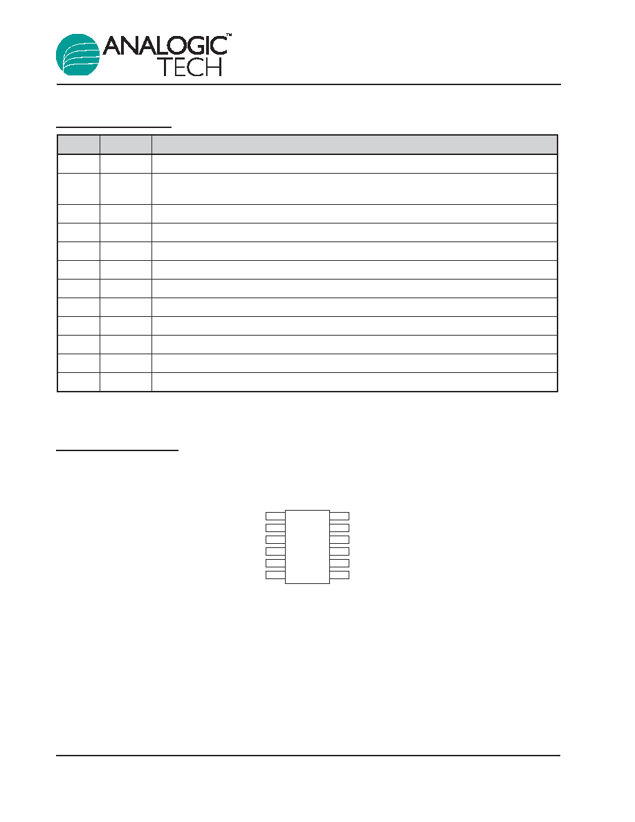
Pin Descriptions
Pin Configuration
TSOPJW-12
(Top View)
1
2
3
4
5
6
12
11
10
9
8
7
C2+
CP
C1-
C1+
ISRC
EN/SET
C2-
IN
GND
DR
DG
DB
Pin # Symbol
Function
1
C2+
Flying capacitor 2 positive terminal. Connect a 1µF capacitor between C2+ and C2-.
2
CP
Charge pump output. Requires 1µF capacitor connected between this pin and
ground.
3
C1-
Flying capacitor 1 negative terminal.
4
C1+
Flying capacitor 1 positive terminal. Connect a 1µF capacitor between C1+ and C1-.
5
ISRC
Current source output.
6
EN/SET
AS
2
Cwire control pin.
7
DB
Open drain switch blue diode cathode.
8
DG
Open drain switch green diode cathode.
9
DR
Open drain switch red diode cathode.
10
GND
Ground.
11
IN
Input power supply. Requires 1µF capacitor connected between this pin and ground.
12
C2-
Flying capacitor 2 negative terminal.
AAT3129
High Efficiency 1X/1.5X/2X Charge Pump
for RGB Color LED Applications
2
3129.2005.11.1.3
Absolute Maximum Ratings
1
Thermal Information
Symbol
Description
Value
Units
P
D
Maximum Power Dissipation
2, 3
625
mW
JA
Thermal Resistance
160
∞C/W
Symbol
Description
Value
Units
V
IN
Input Voltage
-0.3 to 6
V
V
CP
Charge Pump Output
-0.3 to 6
V
V
EN/SET
EN/SET to GND Voltage
-0.3 to 6
V
V
EN/SET(MAX)
Maximum EN/SET to Input Voltage
0.3
V
T
J
Operating Junction Temperature Range
-40 to 150
∞C
T
LEAD
Maximum Soldering Temperature (at leads, 10 sec)
300
∞C
AAT3129
High Efficiency 1X/1.5X/2X Charge Pump
for RGB Color LED Applications
3129.2005.11.1.3
3
1. Stresses above those listed in Absolute Maximum Ratings may cause permanent damage to the device. Functional operation at condi-
tions other than the operating conditions specified is not implied. Only one Absolute Maximum Rating should be applied at any one time.
2. Mounted on an FR4 board.
3. Derate 6.25mW/∞C above 25∞C.

Electrical Characteristics
1
V
IN
= 3.5V, C
IN
= C
CP
= C1 = C2 = 1µF; T
A
= -40∞C to +85∞C. Unless otherwise noted, typical values are T
A
= 25∞C.
Symbol
Description
Conditions
Min
Typ
Max
Units
Input Power Supply
V
IN
Operation Range
2.7
5.5
V
I
CC
Operating Current
3.0
V
IN
5.5, CP = 1.5X,
1
3
mA
No Load Current
I
SHDN
Shutdown Current
EN = 0
1
µA
I
SRC
Output Current Accuracy
3.0
V
IN
5.5
-5
5
%
Charge Pump
T
S
Start-Up Delay Time
200
µs
F
CLK
Clock Frequency
1
MHz
Efficiency
V
IN
= 3.5V
93
%
Switches
R
DS(ON)
Switch On Resistance
V
IN
= 3.5V, T
A
= 25∞C
1.5
EN/SET
V
EN(L)
Enable Threshold Low
V
IN
= 2.7V
0.4
V
V
EN(H)
Enable Threshold High
V
IN
= 5.5V
1.4
V
T
EN/SET LO
EN/SET Low Time
0.3
75
µs
T
EN/SET HI MIN
Minimum EN/SET High Time
50
ns
T
OFF
EN/SET Off Timeout
500
µs
T
LAT
EN/SET Latch Timeout
500
µs
I
EN/SET
EN/SET Input Leakage
V
EN/SET
= 5.5V, V
IN
= 5.5V
-1
1
µA
AAT3129
High Efficiency 1X/1.5X/2X Charge Pump
for RGB Color LED Applications
4
3129.2005.11.1.3
1. The AAT3129 is guaranteed to meet performance specifications over the -40∞C to +85∞C operating temperature range and is assured
by design, characterization, and correlation with statistical process controls.

Typical Characteristics
Turn-Off from 1.5X Mode
(V
IN
= 3.6V; Addr = 2; Data = 16)
100
µ
µs/div
EN/SET
(2V/div)
I
ISRC
(50mA/div)
V
ISRC
(2V/div)
Turn-On to 2X Mode
(V
IN
= 2.8V; ISRC = 60mA)
100
µ
µs/div
EN/SET
(2V/div)
CP
(2V/div)
I
ISRC
(50mA/div)
Turn-On to 1.5X Mode
(V
IN
= 3.6V; ISRC = 60mA)
100
µ
µs/div
EN/SET
(2V/div)
CP
(2V/div)
I
ISRC
(50mA/div)
Turn-On to 1X Mode
(V
IN
= 4.2V; ISRC = 60mA)
100
µ
µs/div
EN/SET
(2V/div)
CP
(2V/div)
I
ISRC
(50mA/div)
AAT3129
High Efficiency 1X/1.5X/2X Charge Pump
for RGB Color LED Applications
3129.2005.11.1.3
5