 | –≠–Ľ–Ķ–ļ—ā—Ä–ĺ–Ĺ–Ĺ—č–Ļ –ļ–ĺ–ľ–Ņ–ĺ–Ĺ–Ķ–Ĺ—ā: AAT3166 | –°–ļ–į—á–į—ā—Ć:  PDF PDF  ZIP ZIP |
General Description
The AAT3166 is a low noise, constant frequency
charge pump DC/DC converter that uses a tri-
mode load switch (1X), fractional (1.5X), and dou-
bling (2X) conversion to maximize efficiency for
white LED applications. The AAT3166 is capable of
driving four LEDs for a total of 108mA from a 2.7V
to 5.5V input. The current sinks may be operated
individually or in parallel for driving higher-current
LEDs. A low external parts count (two 1ĶF flying
capacitors and two small 1ĶF capacitors at IN and
OUTCP) make this part ideally suited for small,
battery-powered applications.
AnalogicTech's AS
2
CwireTM (Advanced Simple Serial
ControlTM) serial digital input is used to enable, dis-
able, and set current for each LED with a 16-level
logarithmic scale plus four low-current settings down
to 115ĶA. For optimized efficiency, low-current set-
tings require only 50ĶA of housekeeping current.
Each output of the AAT3166 is equipped with built-
in protection for output short-circuit and auto-dis-
able for load short-circuit condition. Built-in soft-
start circuitry prevents excessive inrush current
during start-up. A low-current shutdown feature dis-
connects the load from the input and reduces qui-
escent current to less than 1ĶA.
The AAT3166 is available in a Pb-free, space sav-
ing, 3
◊3mm TDFN33-12 package and is rated over
the -40įC to +85įC temperature range.
Features
∑
V
IN
Range: 2.7V to 5.5V
∑
Fully Programmable Current with Single Wire
-- 16-Step Logarithmic Scale
-- 14/18/27mA Max Current
-- Four Low-Current Settings Down to 115ĶA
-- Low I
Q
(50ĶA) for Single-Channel, Low-
Current Mode
∑
Tri-Mode 1X, 1.5X, 2X Charge Pump for
Maximum Efficiency and V
F
Coverage
∑
Drives Up to Four LEDs
∑
Individual Main-Sub (3-1) Group Control
∑
No Inductors, Low Noise Operation
∑
1MHz Constant Switching Frequency
∑
Small Application Circuit
∑
Built-In Thermal Protection
∑
Built-In Auto-Disable for Open Circuit
∑
Automatic Soft Start
∑
I
Q
<1uA in Shutdown
∑
TDFN33-12 Package
Applications
∑
Color (RGB) Lighting
∑
Programmable Current Sink
∑
Transmissive LCD Display
∑
White LED Backlighting
∑
White Photo Flash for Digital Still Cameras
AAT3166
High Efficiency 1X/1.5X/2X Charge
Pump for White LED Applications
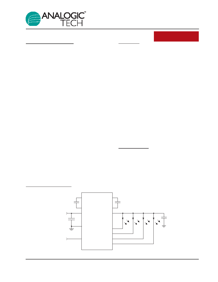
Typical Application
2.7V to 5.5V
EN/SET
IN
EN/SET
C2+
C2-
C1+
C1-
OUTCP
D1
D2
D3
GND
AAT3166
C
IN
1
F
D1
C1
1
F
C2
1
F
D2
D3
D4
C
OUT
1
F
D4
3166.2006.05.1.2
1
ChargePump
TM
Pin Descriptions
Pin Configuration
TDFN33-12
(Top View)
D4
EN/SET
C1+
1
C1-
OUTCP
C2+
D3
D2
D1
GND
IN
C2-
2
3
4
5
6
12
11
10
9
8
7
Pin #
Symbol
Function
1
D4
Current sink input #4.
2
EN/SET
AS
2
Cwire serial interface control pin.
3
C1+
Flying capacitor 1 positive terminal. Connect a 1ĶF capacitor between C1+ and C1-.
4
C1-
Flying capacitor 1 negative terminal.
5
OUTCP
Charge pump output to drive load circuit. Requires 1ĶF capacitor connected between this
pin and ground.
6
C2+
Flying capacitor 2 positive terminal. Connect a 1ĶF capacitor between C2+ and C2-.
7
C2-
Flying capacitor 2 negative terminal.
8
IN
Input power supply. Requires 1ĶF capacitor connected between this pin and ground.
9
GND
Ground.
10
D1
Current sink input #1.
11
D2
Current sink input #2.
12
D3
Current sink input #3.
EP
Exposed paddle; connect to ground as closely as possible to package.
AAT3166
High Efficiency 1X/1.5X/2X Charge
Pump for White LED Applications
2
3166.2006.05.1.2
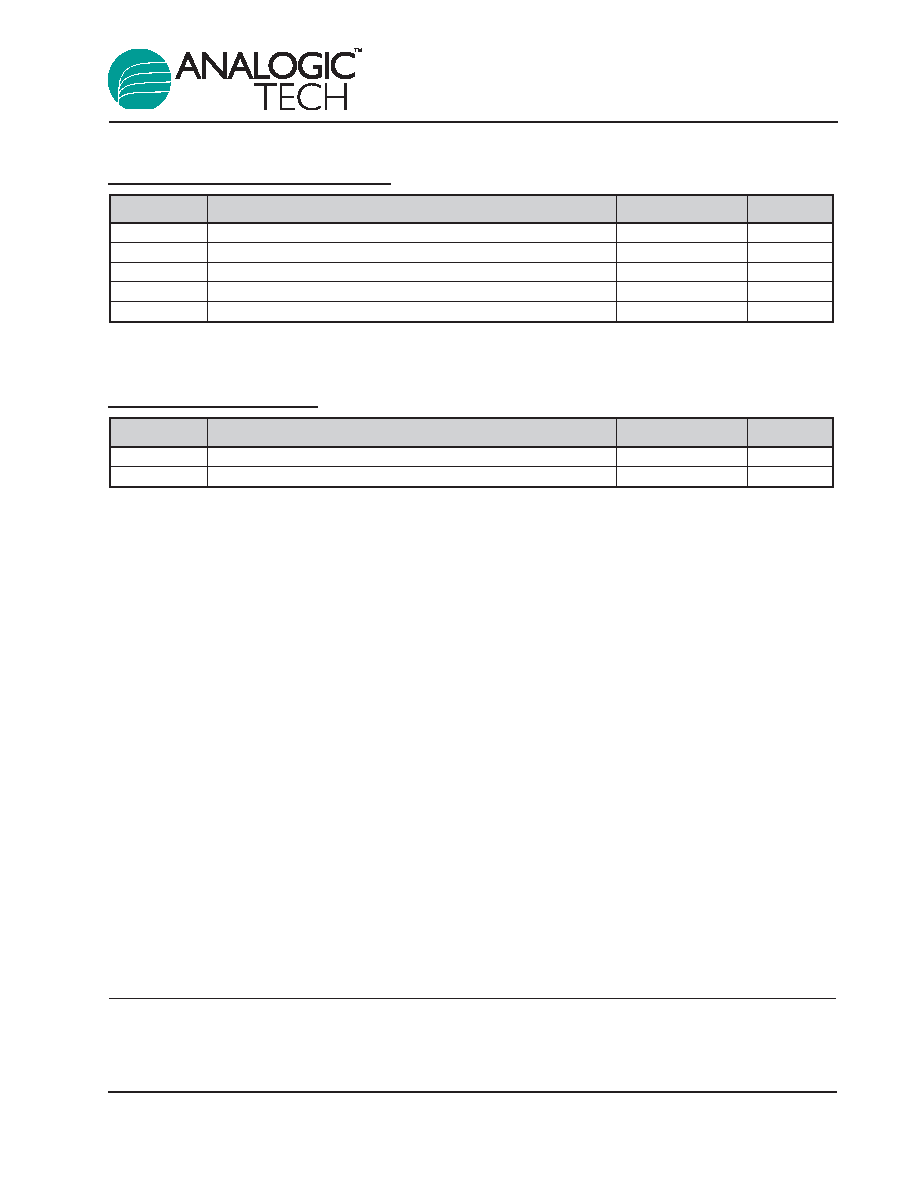
Absolute Maximum Ratings
1
Thermal Information
3
Symbol
Description
Value
Units
P
D
Maximum Power Dissipation
4
2.0
W
JA
Maximum Thermal Resistance
50
įC/W
Symbol
Description
Value
Units
V
IN
Input Voltage to GND
-0.3 to 6
V
V
EN/SET
EN/SET Voltage to GND
-0.3 to V
IN
+ 0.3
V
I
OUT
2
Maximum DC Output Current
150
mA
T
J
Operating Junction Temperature Range
-40 to 150
įC
T
LEAD
Maximum Soldering Temperature (at leads, 10 sec)
300
įC
AAT3166
High Efficiency 1X/1.5X/2X Charge
Pump for White LED Applications
3166.2006.05.1.2
3
1. Stresses above those listed in Absolute Maximum Ratings may cause permanent damage to the device. Functional operation at conditions
other than the operating conditions specified is not implied. Only one Absolute Maximum Rating should be applied at any one time.
2. Based on long-term current density limitation.
3. Mounted on an FR4 board.
4. Derate 20mW/įC above 25įC.
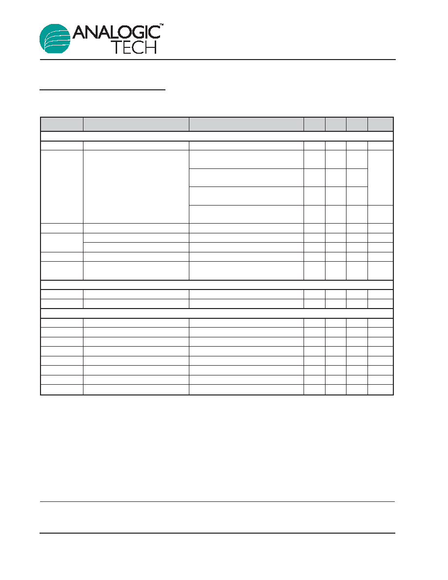
Electrical Characteristics
1
C
IN
= C
OUT
= C
1
= C
2
= 1.0ĶF; T
A
= -40įC to +85įC, unless otherwise noted. Typical values are at T
A
= 25įC,
V
IN
= 3.6V.
Symbol
Description
Conditions
Min
Typ Max Units
Input Power Supply
V
IN
Operation Range
2.7
5.5
V
1X Mode, 3.0
V
IN
5.5, Active,
0.3
No Load Current, High Current Mode
1.5X Mode, 3.0
V
IN
5.5, Active,
1
mA
I
CC
Operating Current
No Load Current, High Current Mode
2X Mode, 3.0
V
IN
5.5, Active,
1
No Load Current, High Current Mode
1X Mode, 3.0
V
IN
5.5, Active,
50
ĶA
No Load Current, Low Current Mode
I
SHDN
Shutdown Current
V
EN/SET
= 0V
1
ĶA
I
DX
High Current Accuracy
I
SET
= 18mA, T
A
= 25įC
-10
10
%
Low Current Accuracy
I
SET
= 400ĶA, T
A
= 25įC
15
%
I
(D-Match)
Current Matching
2
V
F
:D1:D4 = 3.6V
0.5
1
%
V
TH
1X to 1.5X or 1.5X to 2X Transition
150
mV
Threshold at Any I
SINK
Pin
Charge Pump Section
T
SS
Soft-Start Time
100
Ķs
F
CLK
Clock Frequency
1000
kHz
EN/SET
V
EN(L)
Enable Threshold Low
V
IN
= 2.7V
0.4
V
V
EN(H)
Enable Threshold High
V
IN
= 5.5V
1.4
V
T
EN/SET LO
EN/SET Low Time
0.3
75
Ķs
T
EN/SET_HI_MIN
Minimum EN/SET High Time
50
ns
T
EN/SET_HI_MAX
Maximum EN/SET High Time
75
Ķs
T
OFF
EN/SET Off Timeout
500
Ķs
T
LAT
EN/SET Latch Timeout
500
Ķs
I
EN/SET
EN/SET Input Leakage
-1
1
ĶA
AAT3166
High Efficiency 1X/1.5X/2X Charge
Pump for White LED Applications
4
3166.2006.05.1.2
1. The AAT3166 is guaranteed to meet performance specifications over the -40įC to +85įC operating temperature range and is assured
by design, characterization, and correlation with statistical process controls.
2. Current matching is defined as the deviation of any sink current from the average of all active channels.
Typical Characteristics
Unless otherwise noted, V
IN
= 3.5V, C
IN
= C
OUT
= C
1
= C
2
= 1ĶF, T
A
= 25įC.
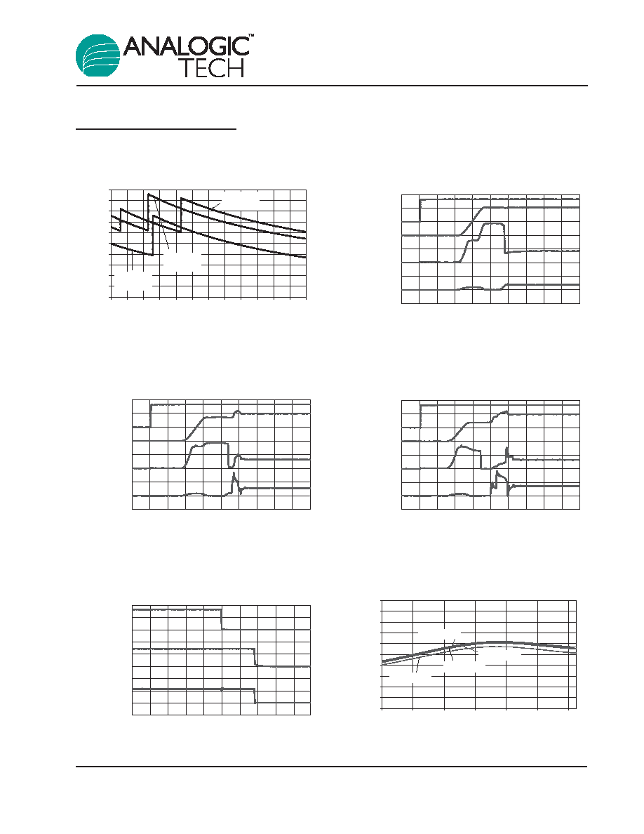
Current Matching vs. Temperature
Temperature (
į
įC)
Current (mA)
17.0
17.2
17.4
17.6
17.8
18.0
18.2
18.4
18.6
18.8
19.0
-40
-20
0
20
40
60
80
Channel 1
Channel 4
Channel 3
Channel 2
Turn-Off from 1.5X Mode
(V
IN
= 3.5V; 18mA Load)
100
s/div
EN
(2V/div)
I
IN
(100mA/div)
V
F
(1V/div)
Turn-On to 2X Mode
(V
IN
= 2.8V; 18mA Load)
100
s/div
EN
(2V/div)
V
OUT
(2V/div)
I
IN
(200mA/div)
V
SINK
(500mV/div)
Turn-On to 1.5X Mode
(V
IN
= 3.5V; 18mA Load)
100
s/div
EN
(2V/div)
V
OUT
(2V/div)
I
IN
(200mA/div)
V
SINK
(500mV/div)
Turn-On to 1X Mode
(V
IN
= 4.2V; 18mA Load)
100
s/div
EN
(2V/div)
V
OUT
(2V/div)
I
IN
(200mA/div)
V
SINK
(500mV/div)
Efficiency vs. Supply Voltage
Supply Voltage (V)
Efficiency (%)
0
10
20
30
40
50
60
70
80
90
100
2.5 2.8 3.0 3.3 3.5 3.8 4.0 4.3 4.5 4.8 5.0 5.3 5.5
5.1mA
V
F
= 3.0V
350A
V
F
= 2.7V
18mA
V
F
= 3.4V
AAT3166
High Efficiency 1X/1.5X/2X Charge
Pump for White LED Applications
3166.2006.05.1.2
5