
AAT3170
High Current LED Flash Driver Charge Pump IC
3170.2006.10.1.0
1
ChargePump
TM
General Description
The AAT3170 is a high output current, high effi-
ciency, low noise, low profile charge pump DC/DC
converter, ideal for multi-function LED photo-flash
applications where solution cost, size, and efficien-
cy are critical.
The dual charge pump in the AAT3170 is capable
of delivering 600mA output current. Two current-
controlled paths are available for users of dual
flash LEDs that prefer current matching. Each LED
channel can be easily programmed in 32 steps with
a single GPIO output through the AS
2
CwireTM
(Advanced Simple Serial ControlTM) interface. This
allows smooth transitions and flexible adjustment
of brightness in flash or other lighting modes.
The tri-mode (1X/1.5X/2X) operation of the internal
charge pump offers excellent power efficiency for
both flash and movie modes. Combined with a low
external parts count (two 1µF flying capacitors and
one small bypass capacitor at V
IN
and OUT), the
AAT3170 is ideally suited for small, battery-powered
applications.
The AAT3170 has a thermal management system to
protect the device in the event of a short-circuit con-
dition at the output pin. Built-in soft-start circuitry
prevents excessive inrush current during start-up.
The shutdown feature disconnects the load from V
IN
and reduces quiescent current to less than 1.0µA.
The AAT3170 is available in the Pb-free, thermally-
enhanced, 12-pin 3x3mm TDFN package.
Features
∑
V
IN
Range: 2.7V to 5.5V
∑
600mA Output Current
∑
Tri-Mode 1X/1.5X/2X in Current Mode
∑
Voltage Mode Operation: 1.5X, 200mA
∑
Dual Regulated Current Sinks
∑
Current Match Between Current Sinks
∑
32 Current Steps Set by AS
2
Cwire
∑
1µF Input, Output, and Flying Capacitors
∑
<1.0µA of Shutdown
∑
Small Application Circuit
∑
No Inductors
∑
Automatic Soft Start
∑
12-Pin TDFN 3x3mm Package
∑
-40∞C to +85∞C Temperature Range
Applications
∑
Camera Phones
∑
Digital Still Cameras (DSCs)
∑
PDAs and Notebook PCs
∑
Smart Phones
Typical Application
AAT3170
C
OUT
2.2µF
EN/SET
VIN
C1+
C1-
C2+
C2-
VOUT
F1
F2
2.7V to 5.5V
EN/SET
Flash
C
T
0.1µF
LED 1
Flash
LED 2
CT
GND
C
IN
4.7µF
C1
1µF
C2
1µF
AAT3170
High Current LED Flash Driver Charge Pump IC
2
3170.2006.10.1.0
Pin Descriptions
Pin Configuration
TDFN33-12
(Top View)
VIN
C1+
C1-
1
GND
F1
F2
VIN
VOUT
C2+
C2-
CT
EN/SET
2
3
4
5
6
12
11
10
9
8
7
Pin #
Symbol
Function
1, 12
VIN
Input power supply pin. Requires 4.7µF bypass capacitor to ground.
2
C1+
Flying capacitor C1 positive terminal. Connect a 1.0µF capacitor between C1+ and C1-.
3
C1-
Flying capacitor C1 negative terminal.
4
GND
Ground connection.
5
F1
Current sink input #1.
6
F2
Current sink input #2.
7
EN/SET
AS
2
Cwire serial interface control pin.
8
CT
Flash timer control capacitor input. Connect a 100nF capacitor from CT to GND for a one
second timeout duration.
9
C2-
Flying capacitor C2 negative terminal.
10
C2+
Flying capacitor C2 positive terminal. Connect a 1µF capacitor between C2+ and C2-.
11
VOUT
Charge pump output. Requires 2.2µF capacitor connected between this pin and ground.
EP
Exposed paddle (bottom); connect to GND directly beneath package.
AAT3170
High Current LED Flash Driver Charge Pump IC
3170.2006.10.1.0
3
Absolute Maximum Ratings
1
T
A
= 25∞C, unless otherwise noted.
Thermal Information
2
Symbol
Description
Value
Units
JA
Maximum Thermal Resistance
50
∞C/W
P
D
Maximum Power Dissipation
2.0
W
Symbol
Description
Value
Units
V
IN
Input Voltage
-0.3 to 6.0
V
V
EN
EN to GND Voltage
-0.3 to 6.0
V
V
EN(MAX)
Maximum EN to Input Voltage
V
IN
+ 0.3
V
I
OUT
Maximum DC Output Current
700
mA
T
J
Operating Junction Temperature Range
-40 to 150
∞C
T
S
Storage Temperature Range
-65 to 150
∞C
T
LEAD
Maximum Soldering Temperature (at leads, 10 sec)
300
∞C
1. Stresses above those listed in Absolute Maximum Ratings may cause permanent damage to the device. Functional operation at condi-
tions other than the operating conditions specified is not implied. Only one Absolute Maximum Rating should be applied at any one time.
2. Mounted on an FR4 board.
AAT3170
High Current LED Flash Driver Charge Pump IC
4
3170.2006.10.1.0
Electrical Characteristics
1
C
IN
= 4.7µF, C
OUT
= 2.2µF, C
1
= C
2
= 1.0µF; T
A
= -40∞C to +85∞C, unless otherwise noted. Typical values are
T
A
= 25∞C, V
IN
= 3.6V.
Symbol
Description
Conditions
Min Typ Max Units
Power Supply
V
IN
Input Voltage Range
2.7
5.5
V
ON/OFF Standby Mode, Code
10
Address = 4, Data = 2
µA
I
CC
Operating Current
1X, No Load Current
300
3.0
V
IN
5.5, 1.5X Mode, No Load Current
2.0
4.0
mA
3.0
V
IN
5.5, 2X Mode, No Load Current
3.0
6.0
I
SHDN(MAX)
V
IN
Pin Shutdown Current
EN = 0
1.0
µA
I
OUT(MAX)
2
Maximum Output Current
V
F
= 3.6V
600
mA
I
(D-Match)
Current Matching Between
V
IN
= 3.6V, T
A
= 25∞C, 428mA
Outputs; High Current
Code Address = 3, Data = 2;
8
%
Code Address = 0, Data = 4
I
(D-Match)
Current Matching Between
V
IN
= 3.6V, T
A
= 25∞C, 100mA
Outputs; Low Current
Code Address = 3, Data =1;
8
%
Code Address = 0, Data = 1
I
DX
Output Current Accuracy
T
A
= 25∞C, Code 1, HI Scale
270
330
mA
F
CLK
Clock Frequency
1
MHz
V
REG
Voltage Mode Regulation
EN/SET Code Address = 6, Data = 2
4.1
4.5
4.9
V
T
SS
Soft-Start Time
200
µs
EN/SET
V
IL
Enable Threshold Low
V
IN
= 2.7V
0.4
V
V
IH
Enable Threshold High
V
IN
= 5.5V
1.4
V
T
EN/SET LO
EN/SET Low Time
0.3
75
µs
T
EN/SET HI MIN
Minimum EN/SET High Time
50
ns
T
EN/SET HI MAX
Maximum EN/SET High Time
75
µs
T
OFF
EN/SET Off Timeout
500
µs
T
LAT
EN/SET Latch Timeout
500
µs
Input Current
EN/SET Input Leakage
-1
1
µA
1. The AAT3170 is guaranteed to meet performance specifications from 0∞C to 70∞C. Specification over the -40∞C to +85∞C operating
temperature range is assured by design, characterization, and correlation with statistical process controls.
2. Mounted on an FR4 board.
AAT3170
High Current LED Flash Driver Charge Pump IC
3170.2006.10.1.0
5
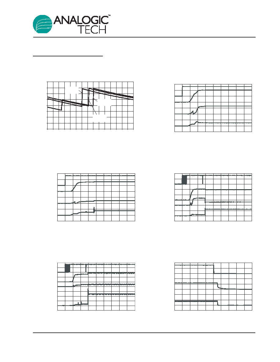
Typical Characteristics
V
IN
= 3.6V, C
IN
= 4.7µF, C
OUT
= 2.2µF, C
1
= C
2
= 1µF, T
A
= 25∞C, unless otherwise noted.
Turn-Off from 1.5X Mode
(V
IN
= 3.2V; 50mA/ch Load)
Time (200µs/div)
EN
(2V/div)
V
F
(1V/div)
I
IN
(200mA/div)
Turn-On to 2X Mode
(V
IN
= 3.2V; 300mA/ch Load)
Time (500µs/div)
EN
(2V/div)
V
OUT
(2V/div)
I
IN
(500mA/div)
V
SINK
(1V/div)
Turn-On to 1X Mode
(V
IN
= 4.2V; 300mA/ch Load)
Time (500µs/div)
EN
(2V/div)
V
OUT
(2V/div)
I
IN
(500mA/div)
V
SINK
(1V/div)
Turn-On to 1.5X Mode
(V
IN
= 3.2V; 50mA/ch Load)
Time (200µs/div)
EN
(2V/div)
V
OUT
(2V/div)
I
IN
(200mA/div)
V
SINK
(1V/div)
Turn-On to 1X Mode
(V
IN
= 4.2V; 50mA/ch Load)
Time (200µs/div)
EN
(2V/div)
V
OUT
(2V/div)
I
IN
(200mA/div)
V
SINK
(1V/div)
Efficiency vs. Supply Voltage
Supply Voltage (V)
Efficiency (%)
20
30
40
50
60
70
80
90
100
2.7 2.8 2.9 3.0 3.1 3.2 3.3 3.4 3.5 3.6 3.7 3.8 3.9 4.0 4.1 4.2
50mA/ch
V
F
= 2.9V
152mA/ch
V
F
= 3.2V
95mA/ch
V
F
= 3.1V