General Description
The AAT3190 charge pump controller provides the
regulated positive and negative voltage biases
required by active matrix thin-film transistor (TFT)
liquid-crystal displays (LCDs), charge-coupled
device (CCD) sensors, and organic light emitting
diodes (OLEDs). Two low-power charge pumps
convert input supply voltages ranging from 2.7V to
5.5V into two independent output voltages.
The dual low-power charge pumps independently
regulate a positive (V
POS
) and negative (V
NEG
) out-
put voltage. These outputs use external diode and
capacitor multiplier stages (as many stages as
required) to regulate output voltages up to ±25V.
Built-in soft-start circuitry prevents excessive in-
rush current during start-up. A high switching fre-
quency enables the use of small external capaci-
tors. The device's shutdown feature disconnects
the load from V
IN
and reduces quiescent current to
less than 1.0µA.
The AAT3190 is available in an MSOP-8 or
TSOPJW-12 package and is specified over the
-40∞C to +85∞C operating temperature range.
Features
∑
V
IN
Range: 2.7V to 5.5V
∑
Adjustable ± Dual Charge Pump
∑
Positive Supply Output Up to +25V
∑
Negative Supply Output Down to -25V
∑
Up to 30mA Output Current
∑
1.0MHz Switching Frequency
∑
<1.0µA Shutdown Current
∑
Internal Power MOSFETs
∑
Internally Controlled Soft Start
∑
Fast Transient Response
∑
Ultra-Thin Solution (No Inductors)
∑
-40∞C to +85∞C Temperature Range
∑
Available in 8-Pin MSOP or 12-Pin TSOPJW
Package
Applications
∑
CCD Sensor Voltage Bias
∑
OLEDs
∑
Passive-Matrix Displays
∑
Personal Digital Assistants (PDAs)
∑
TFT Active-Matrix LCDs
AAT3190
Positive/Negative Charge Pump for Voltage Bias
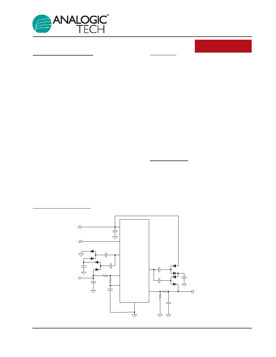
Typical Application
AAT3190
INPUT
NEGATIVE
OUTPUT
POSTIVE
OUTPUT
IN
EN
DRVN
FBN
REF
GND
FBP
DRVP
EN
3190.2005.03.1.0
1
ChargePump
TM

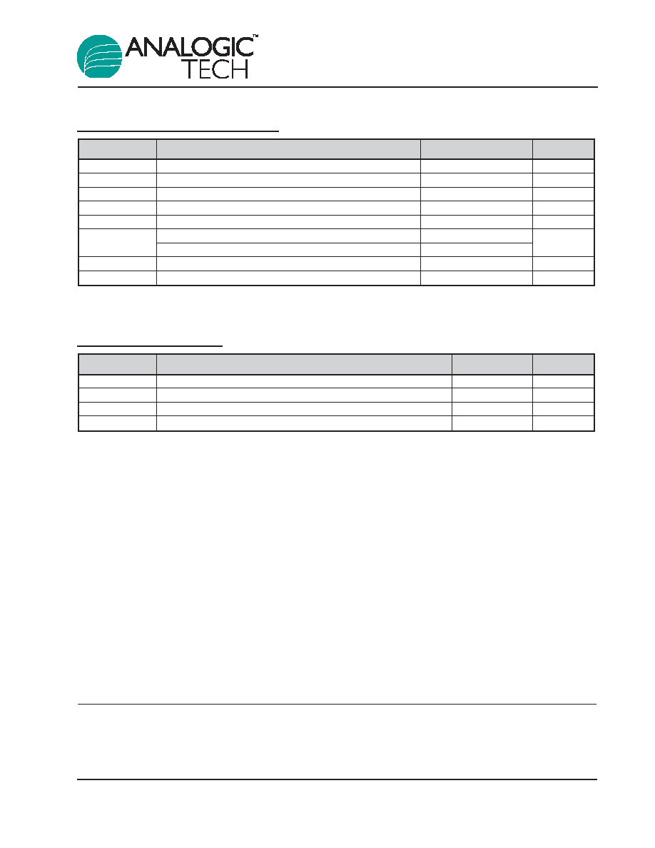
Pin Description
Pin Configuration
MSOP-8
TSOPJW-12
(Top View)
(Top View)
1
2
3
4
5
6
12
11
10
9
8
7
VIN
FBN
REF
EN
FBP
N/C
DRVP
GND
GND
GND
GND
DRVN
1
2
DRVN
VIN
GND
DRVP
FBP
EN
REF
FBN
1
2
3
4
8
7
6
5
Pin #
MSOP-8
TSOPJW-12
Symbol
Function
1
5
FBP
Positive charge pump feedback input. Regulates to 1.2V
nominal. Connect feedback resistive divider to analog
ground (GND).
2
4
EN
Enable input. When EN is pulled low, the device shuts off
and draws only 1.0µA. When high, it is in normal opera-
tion. Drive EN through an external resistor.
3
3
REF
Internal reference bypass terminal. Connect a 0.1µF capac-
itor from this terminal to analog ground (GND). External
load capability to 50µA. REF is disabled in shutdown.
4
2
FBN
Negative charge pump regulator feedback input. Regulates
to 0V nominal. Connect feedback resistive divider to the
reference (REF).
5
12
DVRP
Positive charge pump driver output. Output high level is V
IN
and low level is PGND.
6
8, 9, 10, 11
GND
Ground.
7
7
DRVN
Negative charge pump driver output. Output high level is
V
IN
and low level is PGND.
8
1
VIN
Input voltage: 2.7V to 5.5V.
AAT3190
Positive/Negative Charge Pump for Voltage Bias
2
3190.2005.03.1.0
Absolute Maximum Ratings
1
Thermal Information
Symbol
Description
Value
Units
JA
Thermal Resistance (MSOP-8)
2
150
∞C/W
JA
Thermal Resistance (TSOPJW-12)
2
160
∞C/W
P
D
Maximum Power Dissipation (MSOP-8) (T
A
= 25∞C)
2, 3
667
mW
P
D
Maximum Power Dissipation (TSOPJW-12) (T
A
= 25∞C)
2, 4
625
mW
Symbol
Description
Value
Units
V
IN
Input Voltage
-0.3 to 6
V
V
EN
EN to GND
-0.3 to 6
V
V
N_CH
DRVN to GND
-0.3V to (V
IN
+ 0.3V)
V
V
P_CH
DRVP to GND
-0.3V to (V
IN
+ 0.3V)
V
Other Inputs
REF, FBN, FBP to GND
-0.3V to (V
IN
+ 0.3V)
V
I
MAX
Continuous Current Into DRVN, DRVP
±200
mA
All Other Pins
±10
T
J
Operating Junction Temperature Range
-40 to 150
∞C
T
LEAD
Maximum Soldering Temperature (at leads, 10 sec)
300
∞C
AAT3190
Positive/Negative Charge Pump for Voltage Bias
3190.2005.03.1.0
3
1. Stresses above those listed in Absolute Maximum Ratings may cause permanent damage to the device. Functional operation at
conditions other than the operating conditions specified is not implied. Only one Absolute Maximum rating should be applied at any
one time.
2. Mounted on an FR4 board.
3. Derate 6.7mW/∞C above 25∞C.
4. Derate 6.25mW/∞C above 25∞C.
Electrical Characteristics
V
IN
= 5.0V, C
REF
= 0.1µF, T
A
= -40∞C to +85∞C. Unless otherwise noted, typical values are at T
A
= 25∞C.
Symbol
Description
Conditions
Min
Typ
Max
Units
V
IN
Input Supply Range
2.7
5.5
V
UVLO
Input Under-Voltage Threshold
V
IN
Rising
1.8
V
V
IN
Falling, 40mV Hysteresis (typ)
1.6
I
IN
Input Quiescent Supply Current
V
FBP
= 1.5V, V
FBN
= -0.2V,
400
800
µA
No Load on DRVN and DRVP
I
SD
Shutdown Supply Current
V
EN
= 0 V
0.1
1.0
µA
F
OSC
Operating Frequency
0.8
1.0
1.2
MHz
Negative Low-Power Charge Pump
V
FBN
FBN Regulation Voltage
-100
0
+100
mV
I
FBN
FBN Input Bias Current
V
FBN
= -50mV
-100
+100
nA
R
DSNCHN
DRVN NCH On-Resistance
1.5
5.0
R
DSPCHMIN
MIN DRVN PCH On-Resistance
V
FBN
= 100mV, V
IN
= 4V
1.0
5.0
R
DSPCHMAX
MAX DRVN PCH On-Resistance V
FBN
= -100mV, V
IN
= 4V
20
k
Positive Low-Power Charge Pump
V
FBP
FBP Regulation Voltage
1.15
1.2
1.25
V
I
FBP
FBP Input Bias Current
V
FBP
= 1.5V
-60
+100
nA
R
DSPCHP
DRVP PCH On-Resistance
1.0
5.0
R
DSNCHMIN
MIN DRVP NCH On-Resistance
V
FBP
= 1.15V, V
IN
= 4V
3
15
R
DSNCHMIN
MAX DRVP NCH On-Resistance V
FBP
= 1.25V, V
IN
= 4V
20
k
Reference
Reference Voltage
-2.0 µA < I
REF
< 50 µA
1.18
1.2
1.22
V
V
REF
Reference Under-Voltage
V
REF
Rising
0.8
V
Threshold
Logic Signals
V
IL
Input Low Voltage
0.5
V
V
IH
Input High Voltage
1.5
V
I
IL
Enable Input Low Current
V
IN
= 5.0V, F
BP
= 1.5V, F
BN
= -0.2V
1
µ
A
I
IH
Enable Input High Current
V
IN
= 5.0V, F
BP
= 1.5V, F
BN
= -0.2V
1
µ
A
Thermal Limit
T
SD
Over-Temperature Shutdown
140
∞C
Threshold
T
HYST
Over-Temperature Shutdown
15
∞C
Hysteresis
AAT3190
Positive/Negative Charge Pump for Voltage Bias
4
3190.2005.03.1.0
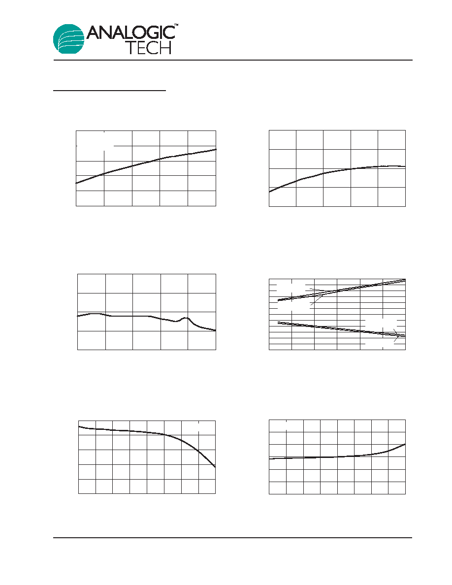
Typical Characteristics
Negative Output Voltage vs. Load Current
(T
A
= 25
∞
∞C)
-8
-7.75
-7.5
-7.25
-7
-6.75
-6.5
0
10
20
30
40
I
NEG
(mA)
V
NEG
(V)
V
IN
= 5.0V
Positive Output Voltage vs. Load Current
(T
A
= 25
∞
∞C)
I
POS
(mA)
V
POS
(V)
11.4
11.6
11.8
12
12.2
12.4
0
5
10
15
20
25
30
35
40
V
IN
= 5.0V
Maximum V
OUT
vs. V
IN
(I
OUT
= 5mA and 15mA)
-15
-12.5
-10
-7.5
-5
-2.5
0
2.5
5
7.5
10
12.5
15
2.5
3
3.5
4
4.5
5
5.5
Input Voltage (V)
Output Voltage (V)
I
ON
= 15mA
I
OP
= 15mA
I
ON
= 5mA
I
OP
= 5mA
Reference Voltage vs. Temperature
1.18
1.19
1.2
1.21
1.22
-40
-15
10
35
60
85
Temperature (
∞C)
Reference Voltage (V)
Switching Frequency vs. Temperature
800
850
900
950
1000
-40
-15
10
35
60
85
Temperature (
∞
∞C)
Frequency (kHz)
Quiescent Current vs. Temperature
250
270
290
310
330
350
-40
-15
10
35
60
85
Temperature (
∞C)
Quiescent Current (
µ
A)
V
FBP
= 1.5V
V
FBN
= -0.2V
AAT3190
Positive/Negative Charge Pump for Voltage Bias
3190.2005.03.1.0
5