
Preliminary
Information
3215.2002.03.0.91
1
General Description
The AAT3215 MicroPowerTM Low Dropout Linear
Regulator is ideally suited for portable applications
where low noise, extended battery life and small
size are critical. The AAT3215 has been specifi-
cally designed for very low output noise perform-
ance, fast transient response and high power sup-
ply rejection ratio (PSRR), making it ideal for pow-
ering sensitive RF circuits.
Other features include low quiescent current, typi-
cally 95µA, and low dropout voltage which is typi-
cally less than 140mV at full output current. The
device is output short circuit protected and has a
thermal shutdown circuit for additional protection
under extreme conditions.
The AAT3215 also features a low-power shutdown
mode for extended battery life. A reference bypass
pin has been provided to improve PSRR perform-
ance and output noise, by connecting an external
capacitor from the AAT3215's reference output to
ground.
The AAT3215 is available in a space saving 5-pin
SOT-23 or 8-pin SC70-JW package in 8 factory
programmed voltages of 2.5V, 2.7V, 2.8V, 2.85V,
2.9V, 3.0V, 3.3V, or 3.5V.
Features
∑
Low Dropout - 140mV at 150mA
∑
Guaranteed 150mA Output
∑
High accuracy ±1.5%
∑
95µA Quiescent Current
∑
High Power Supply Ripple Rejection
∑
70 dB at 1kHz
∑
50 dB at 10kHz
∑
Very low self noise 45µVrms/rtHz
∑
Fast line and load transient response
∑
Short circuit protection
∑
Over-Temperature protection
∑
Uses Low ESR ceramic capacitors
∑
Noise reduction bypass capacitor
∑
Shutdown mode for longer battery life
∑
Low temperature coefficient
∑
8 Factory programmed output voltages
∑
SOT-23 5-pin or SC70-JW 8-pin package
Applications
∑
Cellular Phones
∑
Notebook Computers
∑
Portable Communication Devices
∑
Personal Portable Electronics
∑
Digital Cameras
AAT3215
150mA CMOS High Performance LDO
Typical Application
AAT3215
EN
IN
OUT
BYP
GND
ON/OFF
1
µ
F
10nF
2.2
µ
F
V
IN
GND
GND
V
OUT
PowerLinear
TM
AAT3215
150mA CMOS High Performance LDO
2
3215.2002.03.0.91
Pin Descriptions
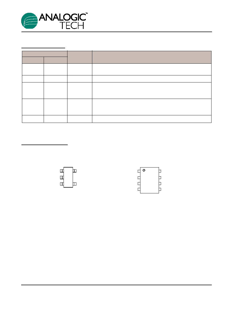
Pin Configuration
SOT-23-5
SC70JW-8
(Top View)
(Top View)
OUT
OUT
OUT
1
2
GND
EN
IN
IN
BYP
1
2
3
4
8
7
6
5
1
2
3
BYP
EN
OUT
4
5
GND
IN
Pin #
Symbol
Function
SOT23-5
SC70JW-8
1
5, 6
IN
Input voltage pin - should be decoupled with 1µF or greater
capacitor.
2
8
GND
Ground connection pin
3
7
EN
Enable pin - this pin is internally pulled high. When pulled low
the PMOS pass transistor turns off and all internal circuitry
enters low-power mode, consuming less than 1µA.
4
1
BYP
Bypass capacitor connection - to improve AC ripple rejection,
connect a 10nF capacitor to GND. This will also provide a soft
start function.
5
2, 3, 4
OUT
Output pin - should be decoupled with 2.2µF capacitor.
AAT3215
150mA CMOS High Performance LDO
3215.2002.03.0.91
3
Absolute Maximum Ratings
(T
A
=25∞C unless otherwise noted)
Note: Stresses above those listed in Absolute Maximum Ratings may cause permanent damage to the device. Functional operation at con-
ditions other than the operating conditions specified is not implied. Only one Absolute Maximum rating should be applied at any one time.
Thermal Information
Note 1: Mounted on a demo board.
Recommended Operating Conditions
Electrical Characteristics
(V
IN
=V
OUT(NOM)
+1V, I
OUT
=1mA, C
OUT
=2.2µF, C
IN
=1µf, C
BYP
=10nF, T
A
=
-40 to 85∞C unless otherwise noted. Typical values are T
A
=25∞C)
Note 1: V
DO
is defined as V
IN
- V
OUT
when V
OUT
is 98% of nominal.
Symbol
Description
Conditions
Min Typ
Max
Units
V
OUT
Output Voltage Tolerance
I
OUT
= 1mA to 150mA
T
A
=25∞C
-1.5
1.5
%
T
A
=-40 to 85∞C -2.5
2.5
%
I
OUT
Output Current
V
OUT
> 1.2V
150
mA
V
DO
Dropout Voltage
1
I
OUT
= 150mA
140
250
mV
I
SC
Short Circuit Current
V
OUT
< 0.4V
600
mA
I
Q
Ground Current
V
IN
= 5V, No load, EN = V
IN
95
150
µA
I
SD
Shutdown Current
V
IN
= 5V, EN = 0V
1
µA
V
OUT
/V
OUT
*
V
IN
Line Regulation
V
IN
= V
OUT
+ 1 to 5.5V
0.07
%/V
V
OUT
(line)
Dynamic Line Regulation
V
IN
=V
OUT
+1V to V
OUT
+2V, I
OUT
=150mA,
1
mV
T
R
/T
F
=2µs
V
OUT
(load)
Dynamic Load Regulation
I
OUT
= 1mA to 150mA, T
R
<5µs
30
mV
V
EN(L)
Enable Threshold Low
0.6
V
V
EN(H)
Enable Threshold High
1.5
V
I
EN
Leakage Current on Enable Pin
V
EN
= 5V
1
µA
1 kHz
70
PSRR
Power Supply Rejection Ratio
I
OUT
=10mA, C
BYP
=10nF
10kHz
50
dB
1MHz
47
T
SD
Over Temp Shutdown Threshold
150
∞C
T
HYS
Over Temp Shutdown Hysteresis
10
∞C
e
N
Output Noise
Noise Power BW = 300Hz-50kHz
45
µVrms/rtHz
TC
Output Voltage Temp. Coeff.
22
ppm/∞C
Symbol
Description
Rating
Units
V
IN
Input Voltage
(V
OUT
+0.3) to 5.5
V
T
Ambient Temperature Range
-40 to +85
∞C
Symbol
Description
Rating
Units
JA
Maximum Thermal Resistance
1
(SOT23-5, SC70JW-8)
190
∞C/W
P
D
Maximum Power Dissipation
1
(SOT23-5, SC70JW-8)
526
mW
Symbol
Description
Value
Units
V
IN
Input Voltage
6
V
I
OUT
DC Output Current
P
D
/(V
IN
-V
O
)
mA
T
J
Operating Junction Temperature Range
-40 to 150
∞C
T
LEAD
Maximum Soldering Temperature (at leads, 10 sec)
300
∞C
Typical Characteristics
(Unless otherwise noted, V
IN
= 5V, T
A
= 25∞C)
Output Voltage vs. Temperature
3.007
3.008
3.009
3.01
3.011
3.012
3.013
3.014
-50
0
50
100
150
Temperature (
∞
C)
Output Voltage
Ground Current vs. Temperature
V
OUT
=3.0V
80
85
90
95
100
105
-50
0
50
100
150
Temperature (
∞
C)
I
GND
(
µ
A)
Ground Current vs. Input Voltage
0
20
40
60
80
100
120
2
3
4
5
V
IN
I
GND
(
µ
A)
V
OUT
=3.0V
I
OUT
=0
I
OUT
=5mA
I
OUT
=150mA
Dropout Voltage vs. Output Current
0
20
40
60
80
100
120
140
160
180
200
0
50
100
150
Output Current (mA)
Dropout Voltage (mV)
Dropout Characteristics
2.7
2.8
2.9
3.0
3.1
2.9
3.0
3.1
3.2
3.3
Vin
I
OUT
=0mA
I
OUT
=10mA
I
OUT
=50mA
I
OUT
=100mA
I
OUT
=150mA
Dropout Voltage vs. Temperature
0
20
40
60
80
100
120
140
160
180
200
-40
-20
0
20
40
60
80
100
120
Temperature (
∞
C)
Dropout Voltage (mV)
I
L
=150mA
I
L
=100mA
I
L
=50mA
AAT3215
150mA CMOS High Performance LDO
4
3215.2002.03.0.91
Typical Characteristics
(Unless otherwise noted, V
IN
= 5V, T
A
= 25∞C)
Power Supply Rejection Ratio vs.
Frequency
0
10
20
30
40
50
60
70
80
90
10
100
1k
10k
100k
1m
10m
Frequency (Hz)
PSRR (dB)
4.7
µ
f
2.2
µ
f
1.0
µ
f
C
OUT
=10
µ
f
I
OUT
=150mA
Short Circuit Current
0
0.2
0.4
0.6
0.8
1
1.2
10ms/div
Isc(A)
Load Transient Response
2.80
2.85
2.90
2.95
3.00
3.05
3.10
100
µ
s/div
V
OUT
-100
0
100
200
300
400
500
I
OUT
(mA)
Line Transient Response
2.98
2.99
3.00
3.01
3.02
3.03
3.04
5
µ
s/div
V
OUT
0
1
2
3
4
5
6
V
IN
On/Off Transient Response
C
BYP
=10nF
5ms/div
EN (2V/div)
V
OUT
(1V/div)
10mA
150mA
On/Off Transient Response
No C
BYP
Capacitor
100
µ
s/div
10mA
150mA
EN (2V/div)
V
OUT
(1V/div)
AAT3215
150mA CMOS High Performance LDO
3215.2002.03.0.91
5