
SmartSwitch
TM
AAT3510/1/2/3/4/5/6/7/8/9
Micropower µP Reset with Watchdog Timer
3510.2004.08.1.4
1
General Description
The AAT351x PowerManagerTM products are
members of AnalogicTechTM's Total Power
Management ICTM product family. This family of
Microprocessor Reset Circuits provides the ulti-
mate in versatility, allowing system designers full
customization of the µP monitor and Reset function
without any additional components. The AAT351x
family offers several combinations of threshold
voltage, watchdog timeout period, reset active peri-
od and output drive configurations, which are all
factory programmed options. All devices are avail-
able in 32 reset threshold voltages from 2.6V up to
5V, with three watchdog timeout periods from
6.3ms to 1600ms and three reset timeouts from
1ms up to 140ms. Available output configurations
are active low push-pull, active low open drain,
active low bi-directional and active high push-pull
The AAT351x family is designed to ignore fast neg-
ative transients on V
DD
and to ensure that Reset
outputs remain valid down to 1V.
The AAT351x family is available in the space saving
5-pin SOT23 surface mount package and is speci-
fied over the -40 to +85∞C temperature range.
Features
∑
Tight voltage tolerance: ±1.5%
∑
Low quiescent current: 5µA
∑
Guaranteed Reset Valid down to 1V
∑
32 voltage options from 2.6V to 5.0V
∑
3 Reset active period options
∑
1ms, 20ms, 140ms
∑
3 Watchdog timeout period options
∑
6.3ms, 102ms, 1600ms
∑
4 output options:
∑
Open drain
∑
Inverting
∑
Non-inverting
∑
Bi-directional
∑
Low Tempco: 100ppm/∞C
∑
5-pin SOT23 package
Applications
∑
Notebook Computers
∑
Portable Electronics
∑
Industrial Controllers
∑
Intelligent Instruments
∑
Critical µP and µC Supply Monitoring
∑
Power-On reset circuits
∑
Embedded Control Systems
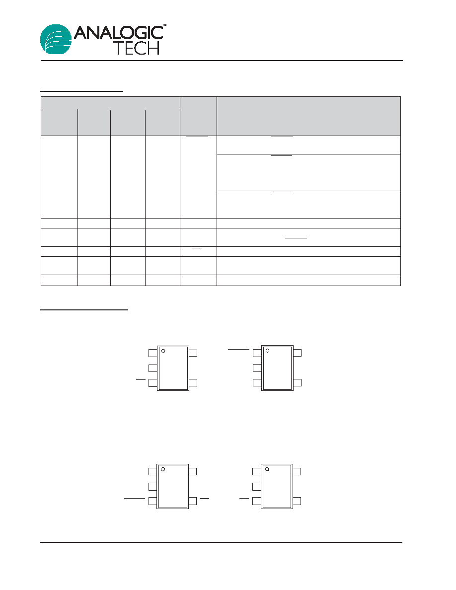
Typical Application
AAT351x
V
CC
RESET
GND
(RESET)
RESET
INPUT
µ
P
V
DD
V
DD
I/O LINE
WDI
PowerManager
TM
AAT3510/1/2/3/4/5/6/7/8/9
Micropower µP Reset with Watchdog Timer
2
3510.2004.08.1.4
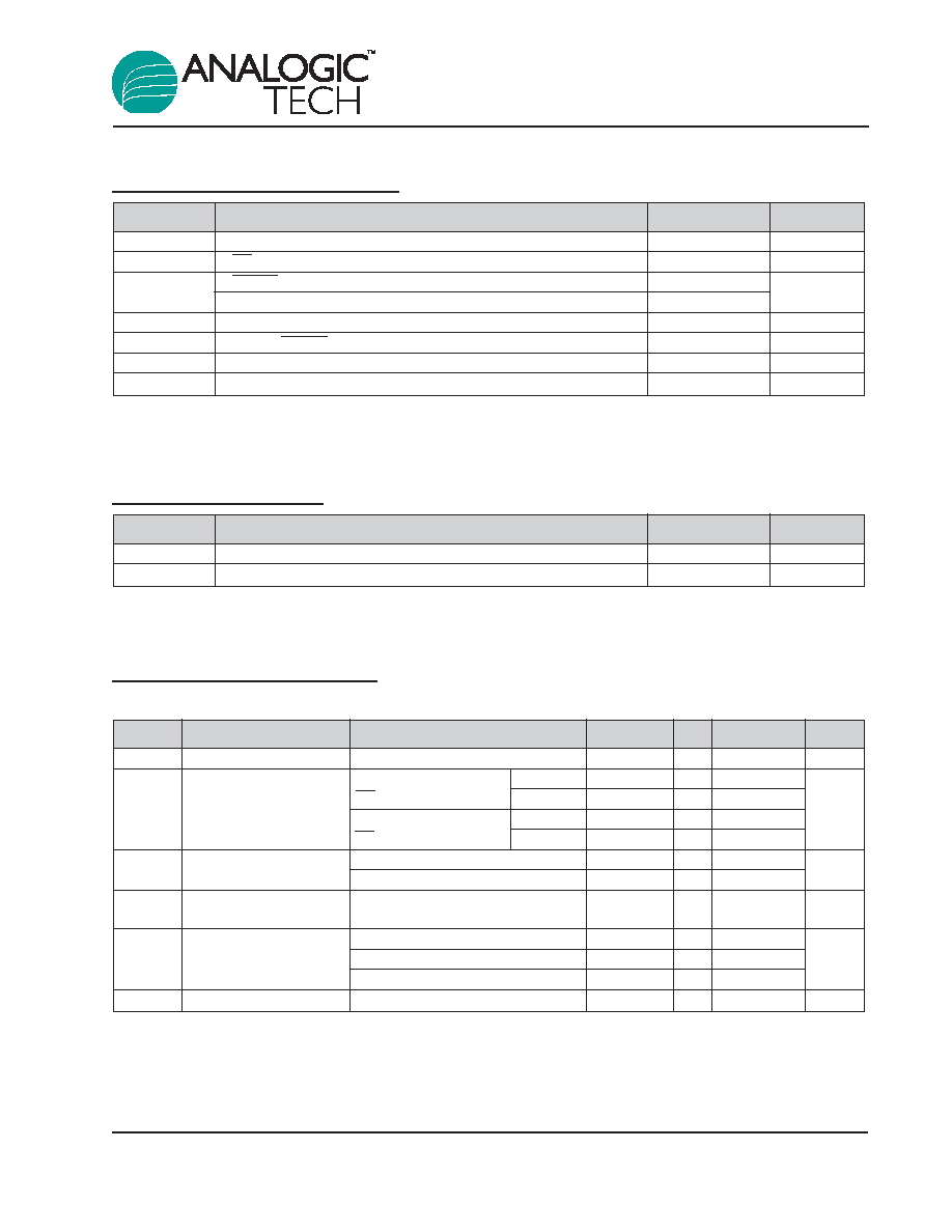
Pin Descriptions
Pin Configuration
(Top View)
AAT3516
AAT3519
(Top View)
AAT3510
AAT3511
(Top View)
AAT3513
AAT3514
AAT3517
AAT3518
(Top View)
AAT3512
AAT3515
5-lead SOT23
5-lead SOT23
5-lead SOT23
5-lead SOT23
GND
V
CC
WDI
MR
RESET
1
2
3
4
5
GND
V
CC
MR
RESET
RESET
1
2
3
4
5
GND
V
CC
WDI
MR
RESET
1
2
3
4
5
GND
V
CC
WDI
RESET
RESET
1
2
3
4
5
Pin #
AAT3510 AAT3512 AAT3513 AAT3515
AAT3511
AAT3514 AAT3516
AAT3517
AAT3518 AAT3519
Symbol
Function
1
N/A
1
1
RESET
AAT3510/13/15: RESET output goes low whenever V
DD
falls below the reset threshold. CMOS push-pull Output
AAT3511/14/16: RESET output goes low whenever V
DD
falls below the reset threshold. Bidirectional CMOS push-
pull Output intended to interface directly to microproces-
sors with bi-directional resets
AAT3517/18/19: RESET output goes low whenever V
DD
falls below the reset threshold. Open drain output. Connect
a pull-up resistor to any supply voltage up to 5.5V
2
2
2
2
GND
Ground connection pin
1
3
3
RESET
RESET active-high output. This CMOS push-pull signal is
the logical inverse of RESET.
3
3
N/A
4
MR
Manual reset input pin. Active low. Pull low to force a reset.
4
4
4
N/A
WDI
Watchdog input pin. Triggers a reset if it remains in a
steady state for the duration of the watchdog timer period.
5
5
5
5
V
CC
Input voltage pin
AAT3510/1/2/3/4/5/6/7/8/9
Micropower µP Reset with Watchdog Timer
3510.2004.08.1.4
3
Absolute Maximum Ratings
(T
A
=25∞C unless otherwise noted)
Note: Stresses above those listed in Absolute Maximum Ratings may cause permanent damage to the device. Functional operation at con-
ditions other than the operating conditions specified is not implied. Only one Absolute Maximum rating should be applied at any one time.
Thermal Information
Note 1: Mounted on FR4 board
Electrical Characteristics
(V
CC
= 2.5V to 5.5V, T
A
= -40 to +85∞C
1
unless otherwise noted.
Typical values are at T
A
=25∞C )
Symbol Description
Conditions
Min
Typ
Max
Units
V
CC
Operating Voltage Range T
A
= -40∞C to +85∞C
1
5.5
V
AAT3510/1/2/3/4/7/8: V
CC
= 3.6V
5
15
MR & WDI unconnected V
CC
= 5.5V
6
18
I
CC
Supply Current
AAT3515/6/9: V
CC
= 3.6V
15
µA
MR unconnected
V
CC
= 5.5V
18
V
TH
Reset Threshold Voltage
T
A
= 25∞C
V
THNOM
-1.5% V
TH
V
THNOM
+1.5%
V
T
A
= -40 to +85∞C
V
THNOM
-2.5% V
TH
V
THNOM
+2.5%
T
C
Reference Voltage
-40∞C < T
A
< +85∞C
±40
ppm/∞C
Temp Coeff
AAT351xIGV-xx-A-x-T1
1
1.4
2
t
RP
Reset Active Timeout
AAT351xIGV-xx-B-x-T1
20
28
40
ms
Period
AAT351xIGV-xx-C-x-T1
140
200
280
T
RD
V
CC
to RESET Delay
V
CC
falling at 1mV/µs
40
µs
Symbol
Description
Value
Units
JA
Maximum Thermal Resistance
1
190
∞C/W
P
D
Maximum Power Dissipation
1
526
mW
Symbol
Description
Max
Units
V
CC
V
CC
to GND
-0.3 to 6
V
V
MR
, V
WDI
MR, WDI to GND
-0.3 to V
CC
+0.3
V
V
RESET
RESET to GND (Push-Pull or Bidirectional Output)
-0.3 to V
CC
+0.3
V
RESET to GND (Open Drain Output)
-0.3 to 6
I
VCC
, I
MR
, I
WDI
Maximum Continuous Input Current
20
mA
I
RESET
RESET/RESET Output Current
20
mA
dV
CC
/dt
Rate of rise of V
CC
100
V/µs
T
J
Operating Junction Temperature Range (-40∞ to 150∞C)
150
∞C

AAT3510/1/2/3/4/5/6/7/8/9
Micropower µP Reset with Watchdog Timer
4
3510.2004.08.1.4
Electrical Characteristics
(V
CC
= 2.5V to 5.5V, T
A
= -40 to +85∫C
1
unless otherwise noted.
Typical values are at T
A
=25∞C )
Symbol Description
Conditions
Min
Typ
Max
Units
Push/Pull RESET Output (AAT3510, 3512, 3513, 3514, 3515, 3516, 3518, 3519)
V
CC
1.0V, I
SINK
= 50µA
0.3
V
CC
1.2V, I
SINK
= 100µA
0.3
V
OL
RESET Low Output Voltage
V
CC
2.7V, I
SINK
= 1.2mA
0.3
V
V
CC
4.5V, I
SINK
= 3.2mA
0.4
V
OH
RESET High Output Voltage
V
CC
2.7V, I
SOURCE
= 500µA
0.8 x V
CC
V
V
CC
4.5V, I
SOURCE
= 800µA
V
CC
- 1.5
V
CC
2.7V, I
SINK
= 1.2mA
0.3
RESET Low Output Voltage
V
CC
4.5V, I
SINK
= 3.2mA
0.4
V
OH
V
CC
1.8V, I
SOURCE
= 150µA
0.8 x V
CC
V
RESET High Output Voltage
V
CC
2.7V, I
SOURCE
= 500µA
0.8 x V
CC
V
CC
4.5V, I
SOURCE
= 800µA
V
CC
- 1.5
Bidirectional RESET Output (AAT3511, 3514, 3516)
t
S
Transition Flip-Flop Setup Time
2
400
ns
V
CC
= 3.0V, C
L
= 120pF
333
t
R
RESET Output Rise Time
3
V
CC
= 5.0V, C
L
= 200pF
333
ns
V
CC
= 3.0V, C
L
= 250pF
666
V
CC
= 5.0V, C
L
= 400pF
666
V
PTH
Active Pullup Enable Threshold
V
CC
= 5.0V
0.4
0.65
V
RESET Active Pullup Current
V
CC
= 5.0V
20
mA
RESET Pullup Resistance
4.2
4.7
5.2
k
Open-Drain RESET Output (AAT3517, 3518, 3519)
V
CC
1.0V, I
SINK
= 50µA
0.3
V
CC
1.2V, I
SINK
= 100µA
0.3
V
OL
RESET Low Output Voltage
V
CC
2.7V, I
SINK
= 1.2mA
0.3
V
V
CC
4.5V, I
SINK
= 3.2mA
0.4
I
D(OFF)
Reset Leakage Current
1.0
µA
Watchdog Input (AAT3510, 3511, 3512, 3513, 3514, 3517, 3518)
AAT351xIGV-xx-x-A-T1
4.3
6.3
9.3
t
WD
Watchdog Timeout Period
AAT351xIGV-xx-x-B-T1
71
102
153
ms
AAT351xIGV-xx-x-C-T1
4
1.12
1.6
2.4
s
t
WDI
WDI Minimum Pulse Width
V
IL
= 0.3 x V
CC
, V
IH
= 0.7 x V
CC
50
ns
V
IL
WDI Input Threshold
5
0.3 x V
CC
V
IH
WDI Input Threshold
5
0.8 x V
CC
V
I
WDI
WDI Input Current
6
WDI = V
CC
, time average
120
160
µA
V
WDI
= 0, time average
-20
-15

AAT3510/1/2/3/4/5/6/7/8/9
Micropower µP Reset with Watchdog Timer
3510.2004.08.1.4
5
Note 1: Over-temperature limits are guaranteed by design, not production tested.
Note 2: This is the minimum time RESET must be held low by an external pulldown source to set the active pullup flip-flop.
Note 3: Measured from RESET V
OL
to (0.8 x V
CC
), Open Circuit Output.
Note 4: Watchdog timeout period C is not available on AAT3513, AAT3514, and AAT3518.
Note 5: WDI is internally serviced within the watchdog period if WDI is left unconnected.
Note 6: The WDI input current is specified as the average input current when the WDI input is driven high or low. The WDI input is
designed for a three-stated-output device with a 10µA maximum leakage current and capable of driving a maximum capacitive load of
200pF. The three-state device must be able to source and sink at least 200µA when active.
Symbol
Description
Conditions
Min
Typ
Max
Units
Manual RESET Input (AAT3510, 3511, 3512, 3515, 3516, 3517, 3519)
V
IL
MR Input Threshold
0.3 x V
CC
V
IH
MR Input Threshold
0.7 x V
CC
V
MR Input Pulse Width
1
µs
MR Glitch Rejection
100
ns
MR Internal Pullup Resistance
T
A
= 25∞C
35
52
75
k
MR to Reset Delay
V
CC
= 5V
230
ns