
AAT3526/7/8
MicroPower Supervisory Circuit with Manual Reset
Typical Application
*AAT3528 Only
AAT3526
AAT3527
AAT3528
uP
V
MR
CC
V
CC
V
CC
RESET
(RESET)
GND
GND
RESET
INPUT
100k
(nominal)
*
Advanced
Information
3526.2002.1.0.62
1
General Description
The AAT3526/7/8 PowerManagerTM products are
members of AATI's Total Power Management ICTM
(TPMICTM) product family. These microprocessor
reset circuits are ideal for monitoring voltage sup-
plies in portable systems, where extended battery
life is critical. They provide a low cost, reliable solu-
tion by eliminating external components. The
AAT3526/7/8 products operate by monitoring the
system power supply voltage. When the input volt-
age drops below a fixed threshold, the device
asserts a reset signal for a minimum of 150ms after
V
CC
has risen back above the fixed threshold. They
are guaranteed to operate down to 1.2V and
designed to ignore fast line transients appearing on
V
CC
. The AAT3526/7/8 series is available with three
output stage versions: AAT3526 push-pull active
low output, AAT3527 push-pull active high output
and AAT3528 open drain active low output. The
quiescent supply current is extremely low, typically
1µA, making this device ideal for portable battery
operated equipment.
The AAT3526/7/8 are available in a 4 pin SOT143
package and are specified over -40∞ to 85∞C oper-
ating temperature range.
Features
∑
1.2V to 5.5V Input voltage range
∑
Operation down to 1.2V
∑
Extremely low quiescent current: less than 2µA
∑
High accuracy detection threshold: ±1.5%
∑
Monitor Power Supply Voltages
∑
Fixed thresholds from 2.2V to 4.6V
∑
Minimum 150ms reset pulse width with fast
delay time <20µs
∑
Debounced Manual Reset Input
∑
Available output configurations:
∑
Open-drain output
∑
CMOS active high output
∑
CMOS active low output
∑
Temp range -40 to 85∞C
∑
4 pin SOT143 package
Applications
∑
Notebook Computers
∑
Cell Phones
∑
Portable Electronics
∑
Embedded Systems
∑
Intelligent Instruments
PowerManager
TM
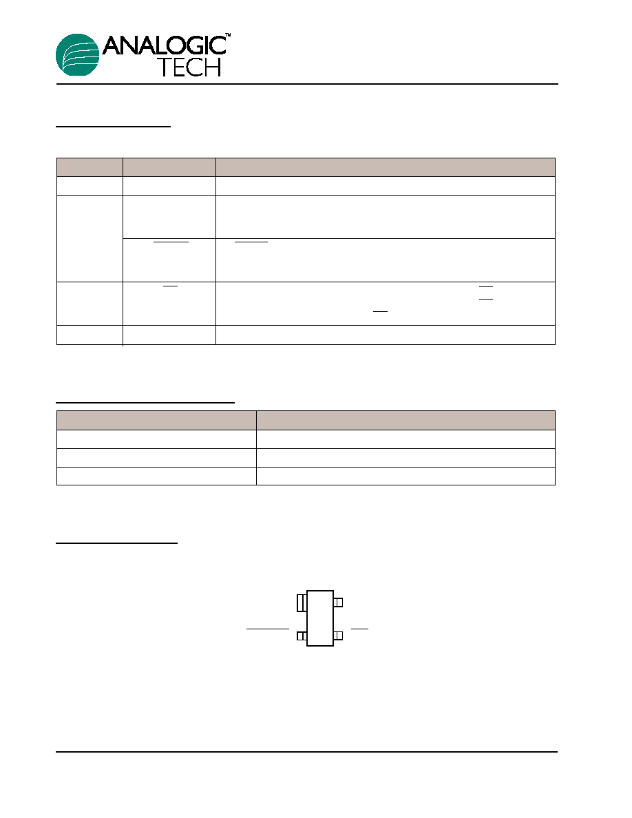
Pin Descriptions
AAT3526, 3527, 3528 (SOT143)
Part Number Descriptions
Pin Configuration
SOT143
(Top View)
1
2
3
4
(RESET) RESET
V
CC
MR
GND
Part Number
Output Type
AAT3526
Reset Output Push Pull Active Low with Delay
AAT3527
Reset Output Push Pull Active High with Delay
AAT3528
Reset Output Open Drain Active Low with Delay
Pin #
Symbol
Function
1
GND
Ground connection
RESET
RESET output remains high while V
CC
is below the reset threshold
2
(AAT3527)
and remains so for a minimum of 150ms after V
CC
raises above the
reset threshold.
RESET
RESET output remains low while V
CC
is below the reset threshold
(AAT3526,
and remains so for a minimum of 150ms after V
CC
raises above the
AAT3528)
reset threshold
3
MR
Manual Reset active low input. A logic low signal on MR asserts a
reset condition. Asserted reset continues as long as MR is low and
for a minimum of 150ms after MR returns high
4
Vcc
Supply Voltage (+1.2V to +5.5V)
AAT3526/7/8
MicroPower Supervisory Circuit with Manual Reset
2
3526.2002.1.0.62

AAT3526/7/8
MicroPower Supervisory Circuit with Manual Reset
3526.2002.1.0.62
3
Absolute Maximum Ratings
(T
A
=25∞C unless otherwise noted)
Note: Stresses above those listed in Absolute Maximum Ratings may cause permanent damage to the device. Functional operation at con-
ditions other than the operating conditions specified is not implied. Only one Absolute Maximum rating should be applied at any one time.
Thermal Information
Note 1: Mounted on an FR4 board.
Symbol
Description
Value
Units
JA
Maximum Thermal Resistance (SOT143)
1
200
∞C/W
P
D
Maximum Power Dissipation (SOT143)
1
320
mW
Symbol
Description
Value
Units
V
CC
V
CC
to GND
-0.3 to 5.5
V
V
MR
MR to GND
-0.3 to V
CC
+0.3
V
V
RESET
RESET to GND (Push-Pull Output)
-0.3 to V
CC
+0.3
V
RESET to GND (Open Drain Output)
-0.3 to 5.5
I
VCC
, I
MR
Maximum Continuous Input Current
20
mA
I
RESET
RESET/RESET Current
20
mA
dVcc/dt
Rate of rise of V
CC
100
V/µs
T
J
Operating Junction Temperature Range
-40 to 150
∞C
T
LEAD
Maximum Soldering Temperature (at Leads) for 10s
300
∞C

AAT3526/7/8
MicroPower Supervisory Circuit with Manual Reset
4
3526.2002.1.0.62
Electrical Characteristics
(V
IN
= 5V, T
A
= -40 to 85∞C unless otherwise noted. Typical values
are at T
A
=25∞C, V
CC
= 5V for 4.63/4.38V versions, V
CC
= 3.3V for 3.08/2.93V versions, V
CC
= 3.0V for 2.63V
versions and V
CC
= 2.5V for 2.32/2.2V versions )
Symbol
Description
Conditions
Min
Typ
Max
Units
V
CC
Operation Voltage
T
A
= 0∫C to +70∫C
1.0
5.5
V
T
A
= -40∫C to +85∫C
1.2
5.5
I
Q
Quiescent Current
V
CC
= 5.5V
1.05
3
µA
V
CC
= 3V
0.85
2
V
TH
RESET Threshold (Table 1)
T
A
= 25∫C
V
TH
-1.5%
V
TH
V
TH
+1.5%
V
T
A
= -40∫C to +85∫C
V
TH
-2.5%
V
TH
V
TH
+2.5%
V
TH
/∞C
RESET Threshold Tempco
40
ppm/∞C
t
P
RESET Propagation Delay
V
CC
= V
TH
to (V
TH
-100mV)
15
µs
t
RDY
RESET Active Timeout Period
150
250
400
ms
t
MR
MR Minimum Pulse Width
10
µs
MRGI
MR Glitch Immunity
100
ns
t
MD
MR to Reset Propagation Delay
0.5
µs
V
IH
MR Input Threshold
V
CC
= V
TH(MAX)
, V
TH
4.38V
2.3
V
V
CC
= V
TH(MAX)
, V
TH
<
4.38V
0.7
◊
V
CC
V
IL
MR Input Threshold
V
CC
= V
TH(MAX)
, V
TH
4.38V
0.8
V
V
CC
= V
TH(MAX)
, V
TH
<
4.38V
0.25
◊
V
CC
R
MR
MR Pull-Up Resistance
10
20
30
k
I
SINK
=1.6mA, V
CC
> 2.1V,
0.3
V
OL
RESET Low Output Voltage
RESET asserted
V
AAT3526, AAT3528
I
SINK
=100µA, V
CC
>1.2V,
0.4
RESET asserted
V
OH
RESET High Output Voltage
I
SOURCE
= 800 µA
V
CC
-1.5
V
AAT3526
I
SINK
=1.2mA, V
CC
> 1.2V,
0.3
V
OL
RESET Low Output Voltage
RESET not asserted
V
AAT3527
I
SINK
= 3.2mA, V
CC
> 4.5V,
0.4
RESET not asserted
I
SOURCE
= 500µA, V
CC
> 2.1V,
0.8V
CC
V
OH
RESET High Output Voltage
RESET asserted
V
AAT3527
I
SOURCE
= 50µA, V
CC
> 1.2V,
0.8V
CC
RESET asserted
I
DOFF
RESET leakage current, AAT3528
V
CC
> V
TH
1
µA
AAT3526/7/8
MicroPower Supervisory Circuit with Manual Reset
3526.2002.1.0.62
5
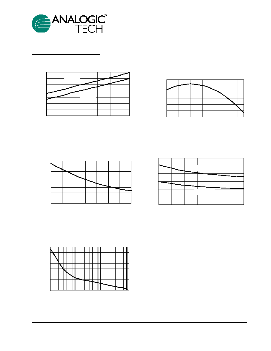
Typical Characteristics
Maximum Transient Duration
vs. Reset Threshold Overdrive
0
50
100
150
200
250
300
350
400
1
10
100
1000
Reset Threshold Overdrive,
V
TH
-V
CC
(mV)
Maximum Transient
Duration (
µ
S)
Power-Down Reset Propagation
Delay vs. Temperature
0
5
10
15
20
25
30
-40
-20
0
20
40
60
80
Temperature (
∞
C)
Reset Propagation Delay (
µ
s)
V
OD
=10mV
V
OD
=100mV
Power-Up Reset Timeout
vs. Temperature
160
180
200
220
240
260
280
300
320
-40
-20
0
20
40
60
80
100
Temperature (
∞
C)
Power-Up Reset
Timeout (ms)
Normalized Reset Threshold
vs. Temperature
0.997
0.998
0.999
1.000
1.001
1.002
1.003
-40
-20
0
20
40
60
80
Temperature (
∞
C)
Normalized Threshold
Supply Current vs. Temperature
0.00
0.20
0.40
0.60
0.80
1.00
1.20
1.40
-40
-20
0
20
40
60
80
Temperature (
∞
C)
Supply Current (
µ
A)
V
CC
=5V
V
CC
=3V