 | –≠–ª–µ–∫—Ç—Ä–æ–Ω–Ω—ã–π –∫–æ–º–ø–æ–Ω–µ–Ω—Ç: AAT3562 | –°–∫–∞—á–∞—Ç—å:  PDF PDF  ZIP ZIP |
AAT3560/2/4
NanoPower Voltage Detector
Preliminary
Information
3560.2002.3.0.91
1
PowerManager
TM
General Description
The AAT3560 Series of PowerManagerTM products
is a member of AATI's Total Power Management
ICTM (TPMICTM) product family. These voltage
detectors are ideal for monitoring voltage supplies
in portable systems, where extended battery life is
critical. They provide a low cost, reliable solution by
eliminating several external components. The
AAT3560 series operates by monitoring the system
power supply voltage. When the input voltage
drops below a fixed threshold, the device output
changes state depending upon configuration.
When the input voltage rises above the threshold,
the device output reverts back to the previous
state. The AAT3560 series are available with three
different output stages: AAT3560 push-pull active
high output, AAT3562 push-pull active low output
and AAT3564 open drain active low output.
The quiescent supply current is extremely low, typ-
ically 1µA , making it ideal for portable battery oper-
ated equipment.
The AAT3560/2/4 are available in a 3 pin SOT-23
package and are specified over -40 to 85∞C oper-
ating temperature range..
Features
∑
1.2V to 5.5V Input voltage range
∑
Operates down to 1.2V
∑
Extremely low quiescent current: less than 2µA
∑
High accuracy detection threshold: ±1.5%
∑
Monitor Power Supply Voltages
∑
Fixed thresholds from 2.2V to 4.6V
∑
Available output configurations:
∑
Open-drain output
∑
CMOS active high output
∑
CMOS active low output
∑
Temp range -40 to 85∞C
∑
3 pin SOT-23 package
Applications
∑
Portable Electronics
∑
Battery Packs
∑
Battery Charger Circuits
∑
Data Acquisition Systems
∑
Power Supplies
∑
Notebook Computers
∑
Intelligent Instruments
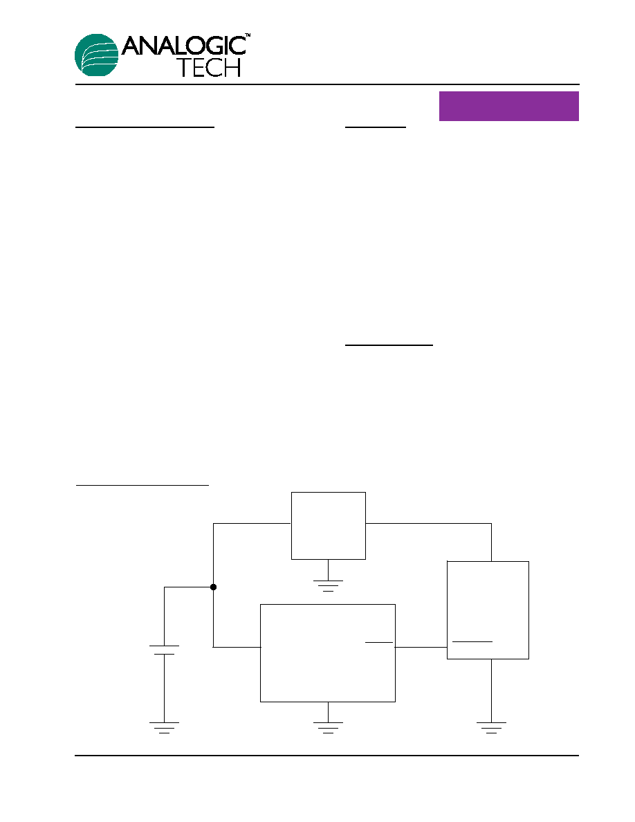
Typical Application
AAT3560
AAT3562
AAT3564
V
CC
V
CC
RESET
(RESET)
GND
SUSPEND
+
Li Ion
µ
P
DC/DC
Converter

Pin Descriptions
AAT3560, 3562, 3564 (SOT23-3)
Part Number Descriptions
Pin Configuration
3-Pin SOT23
(Top View)
1
2
3
(RESET) RESET
V
CC
GND
SOT23-3 Part Number
Part Description
AAT3560
RESET Push Pull Active High
AAT3562
RESET Push Pull Active Low
AAT3564
RESET Open Drain, Active Low
Pin #
Symbol
Function
1
GND
Ground
2
RESET (RESET)
Reset output. See table below for output configurations.
3
V
CC
Supply Voltage (+1.2V to +5.5V)
AAT3560/2/4
NanoPower Voltage Detector
2
3560.2002.3.0.91
AAT3560/2/4
NanoPower Voltage Detector
3560.2002.3.0.91
3
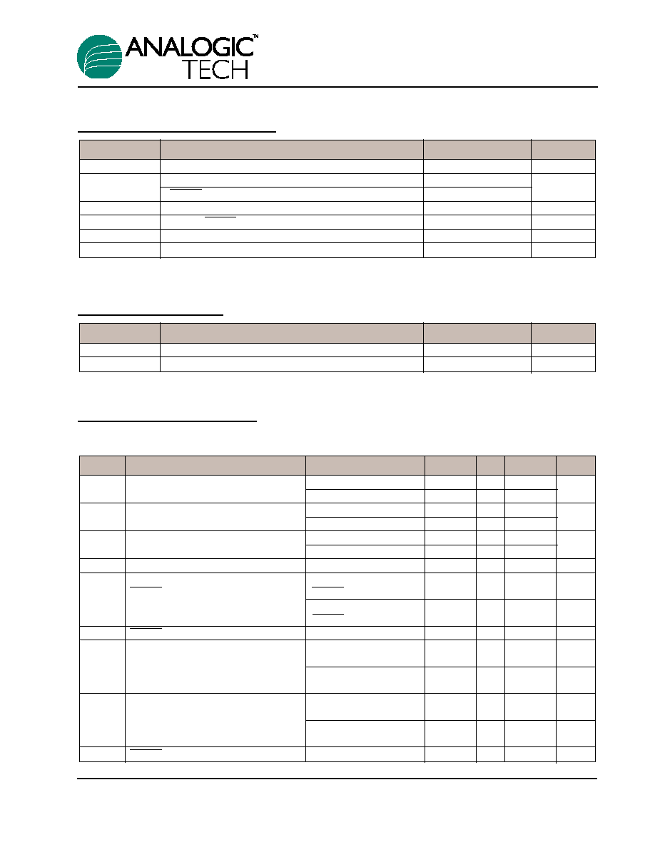
Absolute Maximum Ratings
(T
A
=25∞C unless otherwise noted)
Note: Stresses above those listed in Absolute Maximum Ratings may cause permanent damage to the device. Functional operation at con-
ditions other than the operating conditions specified is not implied. Only one Absolute Maximum rating should be applied at any one time.
Thermal Information
Note 1: Mounted on FR4 board.
Electrical Characteristics
(V
IN
= 5V, T
A
= -40 to 85∞C unless otherwise noted. Typical values
are at T
A
=25∞C, ,V
CC
= 5V for 4.63/4.38V versions, V
CC
= 3.3V for 3.08/2.93V versions, V
CC
= 3.0V for 2.63V
version and V
CC
= 2.5V for 2.32/2.2V versions )
Symbol Description
Conditions
Min
Typ
Max
Units
V
CC
Operation Voltage
T
A
= 0 to 70∫C
1.0
5.5
V
T
A
= -40 to 85∫C
1.2
5.5
I
Q
Quiescent Current
V
CC
= 3V
0.85
2
µA
V
CC
= 5.5V
1.05
3
V
TH
RESET Threshold (Table 1)
T
A
= 25∫ C
V
TH
- 1.5%
V
TH
V
TH
+1.5%
V
T
A
= -40∫C to +85∫C
V
TH
- 2.5%
V
TH
V
TH
+2.5%
dV
T
H/∫C
RESET Threshold Tempco
40
ppm/∞C
I
SINK
=1.6mA, V
CC
> 2.1V,
0.3
V
V
OL
RESET Low Output Voltage
RESET asserted
AAT3562, AAT3564
I
SINK
=100µA, V
CC
>1.2V,
0.4
V
RESET asserted
V
OH
RESET High Output Voltage, AAT3562
I
SOURCE
= 800 µA
V
CC
-1.5
V
I
SINK
=1.2mA, V
CC
> 1.2V,
0.3
V
V
OL
RESET Low Output Voltage
RESET not asserted
AAT3560
I
SINK
= 3.2mA, V
CC
> 4.5V,
0.4
V
RESET not asserted
I
SOURCE
= 500µA, V
CC
>
0.8V
CC
V
V
OH
RESET High Output Voltage
2.1V, RESET asserted
AAT3560
I
SOURCE
= 50µA, V
CC
>
0.8V
CC
V
1.2V, RESET asserted
I
DOFF
RESET Leakage Current, AAT3564
V
CC
> V
TH
1
µA
Symbol
Description
Value
Units
JA
Maximum Thermal Resistance
1
200
∞C/W
P
D
Maximum Power Dissipation
1
320
mW
Symbol
Description
Value
Units
V
CC
V
CC
to GND
-0.3 to 5.5
V
V
RESET
RESET to GND (Push-Pull Output)
-0.3 to V
CC
+0.3
V
RESET to GND (Open Drain Output)
-0.3 to 5.5
I
MAX
Maximum Continuous Input Current
20
mA
I
RESET
RESET/RESET Current
20
mA
T
J
Operating Junction Temperature Range
-40 to 150
∞C
T
LEAD
Maximum Soldering Temperature (at Leads) for 10s
300
∞C

Typical Characteristics
(Unless otherwise noted, V
IN
= 5V, T
A
= 25∞C)
Maximum Transient Duration
vs. Reset Threshold Overdrive
0
50
100
150
200
250
300
350
400
1
10
100
1000
Reset Threshold Overdrive,
V
TH
-V
CC
(mV)
Maximum Transient
Duration (
µ
S)
Power-Down Reset Propagation
Delay vs. Temperature
0
5
10
15
20
25
30
-40
-20
0
20
40
60
80
Temperature (
∞
C)
Reset Propagation Delay (
µ
s)
V
OD
=10mV
V
OD
=100mV
Normalized Reset Threshold
vs. Temperature
0.997
0.998
0.999
1.000
1.001
1.002
1.003
-40
-20
0
20
40
60
80
Temperature (
∞
C)
Normalized Threshold
Supply Current vs. Temperature
0.00
0.20
0.40
0.60
0.80
1.00
1.20
1.40
-40
-20
0
20
40
60
80
Temperature (
∞
C)
Supply Current (
µ
A)
V
CC
=5V
V
CC
=3V
AAT3560/2/4
NanoPower Voltage Detector
4
3560.2002.3.0.91

AAT3560/2/4
NanoPower Voltage Detector
3560.2002.3.0.91
5
Functional Description
General
The AAT3560 series of Nanopower voltage detec-
tors, monitors a system power supply and asserts
an output signal (Low for AAT3562, AAT3564 and
High for AAT3560) when the supply voltage drops
below a factory programmed threshold voltage.
The output signal will remain valid until the input
voltage falls below the Minimum Operating Voltage
of 1V. Below this value the output voltage is unde-
fined. When the input voltage rises above the fac-
tory programmed threshold, the output signal will
resume its inactive state.
Functional Block Diagram
GND
RESET (RESET)
V
REF
V
CC
+
-
+
-
Figure 1. AAT3562 Timing Diagram
V
IN
Ground
Minimum Operating
Voltage
Detection Voltage
Level
Output Voltage
Undefined
Output
Voltage
Ground