
AAT3680
Lithium-Ion Linear Battery Charge Controller
Preliminary Information
3680.2003.4.0.91
1
BatteryManager
TM
Typical Application
Q1
FZT788B
AAT3680
C2
10
µ
F
C1
4.7
µ
F
R2
1k
R
SENSE
0.2
R1
2.5k
BATT+
BATT-
TEMP
RT1
RT2
VP
Battery
Pack
DRV
CSI
VP
VP
VSS
STAT
TS
BAT
T2X
D1
General Description
The AAT3680 BatteryManagerTM is a member of
AnalogicTech's Total Power Management ICTM
family. This device is an advanced Lithium-Ion (Li-
Ion) battery charge and management IC, specifi-
cally designed for low cost compact portable appli-
cations. In a single 8-pin package, the AAT3680
precisely regulates battery charge voltage and
charge current. This device is capable of two trick-
le charge current levels controlled by one external
pin. Battery charge temperature and charge state
are carefully monitored for fault conditions. In the
event of an over current, short circuit or over tem-
perature failure, the device will automatically shut
down, thus protecting the charging device and the
battery under charge. A battery charge state mon-
itor output pin is provided to indicate the battery
charge status though a display LED. The battery
charge status output is a serial interface which may
also be read by a system microcontroller.
The AAT3680 is available in an 8-pin MSOP or 12-
pin TSOPJW package, specified over -20 to 70∞C
range.
Features
∑
4.5V to 15V Input voltage range
∑
1% Accurate Preset Voltages: 4.1V, 4.2V,
8.2V, 8.4V
∑
Low operation current, typically 0.5mA
∑
Programmable Charge Current
∑
Automatic recharge sequencing
∑
Battery temperature monitoring
∑
Deep discharge cell conditioning
∑
Fast trickle charge option with thermal over-ride
∑
Full battery charge auto turn off / sleep mode
∑
Over voltage, current and temperature
protection
∑
Power on reset
∑
LED Charge Status Output or System
Microcontroller serial interface
∑
Temperature range -20 to 70∞C
∑
8 pin MSOP, 12 pin TSOPJW package
Applications
∑
Cellular Phones
∑
Personal Digital Assistants (PDA's)
∑
Desktop Chargers
∑
USB Chargers

Pin Description
Pin Configuration
MSOP-8
TSOPJW-12
(Top View)
(Top View)
1
2
TS
8
7
6
5
CSI
BAT
T2X
NC
VP
VP
VP
VP
STAT
VSS
DRV
1
2
3
4
6
5
5
6
1
2
VP
TS
VSS
STAT
BAT
CSI
T2X
DRV
1
2
3
4
8
7
6
5
Pin #
SOP, TSSOP
MSOP
Symbol
Function
1
7
CSI
Current Sense Input.
2
8
BAT
Battery voltage level sense input.
3
1
VP
Power supply input pin.
4
2
TS
Battery temperature sense input
5
3
STAT
Battery charge status output. Connect an LED in series with 2.2k
from STAT to VP to monitor battery charge state.
6
4
VSS
Common ground connection.
7
5
DRV
Battery charge control output
8
6
T2X
2 x battery trickle charge control input. Connect this pin to VSS to
double the battery trickle charge current. Leave this pin floating for
normal trickle charge current (10% of full charge current). To enter
microcontroller fast-read status, pull this pin high during power-up.
AAT3680
Lithium-Ion Linear Battery Charge Controller
2
3680.2003.4.0.91

Absolute Maximum Ratings
(T
A
=25∞C unless otherwise noted)
Note: Stresses above those listed in Absolute Maximum Ratings may cause permanent damage to the device. Functional operation at con-
ditions other than the operating conditions specified is not implied. Only one Absolute Maximum rating should be applied at any one time.
Note 1: IC devices are inherently ESD sensitive; handling precautions required.
Thermal Information
Note 2: Mounted on an FR4 printed circuit board.
Recommended Operating Conditions
Symbol
Description
Conditions
Min
Typ
Max
Units
V
P
Operation Input Voltage
4.5
15
V
I
DRV
DRV Pin Sink Current
40
mA
T
Ambient Temperature Range
-20
70
∞C
Symbol
Description
Value
Units
JA
Maximum Thermal Resistance (TSOPJW-12)
2
120
∞C/W
JA
Maximum Thermal Resistance (MSOP-8)
2
150
∞C/W
P
D
Maximum Power Dissipation (TSOPJW-12)
2
1.0
W
P
D
Maximum Power Dissipation (MSOP-8)
2
833
mW
Symbol
Description
Value
Units
V
P
V
P
relative to V
SS
-0.3 to 16
V
V
CSI
CSI to GND
-0.3 to V
P
+0.3
V
V
T2X
T2X to GND
-0.3 to 5.5
V
V
BAT
BAT to GND
-0.3 to V
P
+0.3
V
T
J
Operating Junction Temperature Range
-40 to 150
∞C
T
LEAD
Maximum Soldering Temperature (at Leads)
300
∞C
ESD
ESD Rating
Note 1
kV
AAT3680
Lithium-Ion Linear Battery Charge Controller
3680.2003.4.0.91
3

AAT3680
Lithium-Ion Linear Battery Charge Controller
4
3680.2003.4.0.91
Electrical Characteristics
(V
IN
= 4.5V to 15V, T
A
= -20 to 70∞C unless otherwise noted. Typical
values are at T
A
=25∞C)
Note 1: The AAT3680 output charge voltage is specified over 0∞ to 50∞C ambient temperature; operation over -20 to 70∞C is guaranteed
by design.
Symbol Description
Conditions
Min
Typ
Max Units
I
P
Operating Current
V
IN
= 5.5V
0.5
3
mA
I
SLEEP
Sleep Mode Current
V
IN
= 5.5V, V
CH
= 4.1V, V
CH
= 4.2V
2
6
µA
V
CH
= 8.2V, V
CH
= 8.4V
3
10
I
STAT(HI)
STAT high level output
V
IN
= 5.5V
-1
+1
µA
leakage current
V
STAT(LOW)
STAT low level sink current
V
IN
= 5.5V, I
SINK
= 5mA
0.3
0.6
V
I
SINK
DRV pin sink current
V
IN
= 5.5V
20
mA
V
OL@DRV
DRV pin output low
I
SINK
= 5mA, V
IN
= 5.5V
0.4
1.0
V
AAT3680-4.1
T
A
= 25∞C
4.075 4.100
4.125
see note 1
4.059 4.100
4.141
AAT3680-4.2
T
A
= 25∞C
4.175 4.200
4.225
V
CH
Output Charge Voltage
see note 1
4.158 4.200
4.242
V
AAT3680-8.2
T
A
= 25∞C
8.151 8.200
8.249
see note 1
8.118
8.200
8.282
AAT3680-8.4
T
A
= 25∞C
8.350 8.400
8.450
see note 1
8.316 8.400
8.484
V
CS
Charge Current Regulation
V
IN
= 5.5V, V
CH
= 4.1V, V
CH
= 4.2V
90
100
110
mV
V
IN
= 12V, V
CH
= 8.2V, V
CH
= 8.4V
90
100
110
AAT3680-4.1
2.94
3.0
3.06
V
MIN
Preconditioning Voltage Threshold
AAT3680-4.2
3.04
3.1
3.16
V
AAT3680-8.2
5.98
6.1
6.22
AAT3680-8.4
6.08
6.2
6.32
V
TRICKLE
Trickle-Charge Current Regulation
T2X floating
V
CH
= 4.1V, V
CH
= 4.2V
10
mV
V
CH
= 8.2V, V
CH
= 8.4V
10
T
2X
Trickle Charge Current Gain
T2X = V
SS
1.8
V
TS1
Low Temperature Threshold
V
IN
= 15V
29.1
30
30.9
% V
P
V
TS2
High Temperature Threshold
V
IN
= 15V
58.2
60
61.8
% V
P
V
TERM
Charge termination threshold voltage
4
12
24
mV
V
CH
= 4.1V
3.92
4.00
4.08
V
RCH
Battery Recharge Voltage Threshold
V
CH
= 4.2V
4.018
4.10
4.182
V
V
CH
= 8.2V
7.84
8.00
8.16
V
CH
= 8.4V
8.306
8.20
8.364
V
UVLO
Undervoltage Lockout
V
IN
rising, T
A
= 25∞C
3.5
4.0
4.5
V
V
OVP
Over-voltage Protection Threshold
4.4
V
V
OCP
Over-current Protection Threshold
200
% V
CS

AAT3680
Lithium-Ion Linear Battery Charge Controller
3680.2003.4.0.91
5
Functional Block Diagram
LED Signal
Generator
MUX
Microcontroller
Status Generator
Microcontroller
Read Enable
Charge Status
Logic Control
Power-On
Reset
CSI
V
P
STAT
T2X
DRV
V
SS
Under
Voltage
Lock Out
Over Current /
Short Circuit
Protection
2x Trickle
Charge
Control
Loop Select
MUX Driver
BAT
TS
V
REF
Temperature Sense
Comparator
Voltage
Comparator
Current Loop
Error Amp
Voltage Loop
Error Amp
Functional Description
The AAT3680 is a Linear Charge Controller
designed for one and two cell Lithium Ion or
Lithium Polymer batteries. It is a full-featured bat-
tery management system IC with multiple levels of
power savings, system communication and protec-
tion integrated inside. Refer to the block diagram
and flow chart in this section.
Cell Preconditioning
Before starting charging, the AAT3680 checks sev-
eral conditions in order to maintain a safe charging
environment. The input supply must be above the
minimum operating voltage, or undervoltage lock-
out threshold (V
UVLO
), for the charging sequence to
begin. Also, the cell temperature, as reported by a
thermistor connected to TS pin, must be within the
proper window for safe charging. When these con-
ditions have been met, and a battery is connected
to the BAT pin, the AAT3680 checks the state of the
battery. If the cell voltage is below V
MIN
, the
AAT3680 begins preconditioning the cell. This is
performed by charging the cell with 10% of the pro-
grammed constant-current amount. For example if
the programmed charge current is 500mA, then the
preconditioning mode (trickle charge) current will be
50mA. Cell preconditioning is a safety precaution
for deeply discharged cells, and furthermore, limits
the power dissipation in the pass transistor when
the voltage across the device is largest. The
AAT3680 features an optional T2X mode, which
allows faster trickle-charging at approximately two
times the default rate. This mode is selected by
connecting the T2X pin to V
SS
. If an over-tempera-
ture fault is triggered, the fast trickle-charge will be
latched off, and the AAT3680 will continue at the
default 10% charge current.
Constant Current Charging
The cell preconditioning continues until the voltage
on the BAT pin reaches V
MIN
. At this point, the
AAT3680 begins constant-current charging (fast
charging). Current level for this mode is pro-
grammed using a current sense resistor R
SENSE
between V
P
and CSI pins. The CSI pin monitors the
voltage across R
SENSE
to provide feedback for the
current control loop. The AAT3680 remains in con-
stant current charge mode until the battery reaches
the voltage regulation point, V
CH
.

AAT3680
Lithium-Ion Linear Battery Charge Controller
6
3680.2003.4.0.91
Constant Voltage Charging
When the battery's voltage reaches V
CH
during
constant-current mode, the AAT3680 transitions to
constant-voltage mode. The regulation voltage is
factory programmed: 4.1V and 4.2V (or 8.2V and
8.4V for two-cell applications) are available to sup-
port different anode materials in Lithium Ion cells.
In constant-voltage operation, the AAT3680 moni-
tors the cell voltage and terminates the charging
cycle when the voltage across R
SENSE
decreases to
approximately 10mV.
Charge Cycle Termination, Recharge
Sequence
After the charge cycle is complete, the AAT3680
latches off the pass device and automatically enters
power-saving sleep mode. Either of two possible
conditions will bring the IC out of sleep mode: the
battery voltage at the BAT pin drops below V
RCH
(recharge threshold voltage) or the AAT3680 is reset
by cycling the input supply through the power-on
sequence. Falling below V
RCH
signals the IC that it
is time to initiate a new charge cycle.
Figure 1: AAT3680 Operational Flow Chart
UVLO
Temperature Test
TS > V
TS1
TS < V
TS2
Power On Reset
Power On Reset
Preconditioning Test
Current Phase Test
V
CH
> V
BAT
V
MIN
> V
BAT
V
TERM
R
SENSE
< V
RCH
Voltage
Phase Test
V
P
> V
UVLO
Shut Down
Mode
Shut Down
Mode
Yes
No
Yes
Yes
Low Current
Conditioning
Charge
Low Current
Conditioning
Charge
(Trickle Charge)
Temperature
Fault
Temperature
Fault
No
No
Current
Charging
Mode
Current
Charging
Mode
Yes
Voltage
Charging
Mode
Voltage
Charging
Mode
< I
BAT
No
Yes
No
Charge Complete
Latch Off
Charge Complete
Latch Off

AAT3680
Lithium-Ion Linear Battery Charge Controller
3680.2003.4.0.91
7
Sleep Mode
When the input supply is disconnected, the charger
automatically enters power-saving sleep mode. Only
consuming an ultra-low 2µA in sleep mode, the
AAT3680 minimizes battery drain when it is not
charging.This feature is particularly useful in applica-
tions where the input supply level may fall below the
battery charge or under-voltage lockout level. In such
cases where the AAT3680 input voltage drops, the
device will enter the sleep mode and automatically
resume charging once the input supply has recov-
ered from its fault condition. This makes the AAT3680
well suited for USB battery charger applications.
Charge Inhibit
The AAT3680 charging cycle is fully automatic;
however, it is possible to stop the device from
charging even when all conditions are met for
proper charging. Switching the TS pin to either V
P
or V
SS
will force the AAT3680 to turn off the pass
device and wait for a voltage between the low and
high temperature voltage thresholds.
Resuming Charge and the V
RCH
Threshold
The AAT3680 will automatically resume charging
under most conditions when a battery charge cycle is
interrupted. Events such as an input supply interrup-
tion or under voltage, removal and replacement of the
battery under charge or charging a partially drained
battery are all possible. The AAT3680 will monitor the
battery voltage and automatically resume charging in
the appropriate mode based upon the measured bat-
tery cell voltage. The feature is useful for systems
with an unstable input supply which could be the case
when powering a charger from a USB bus supply.
This feature is also beneficial for charging or "topping
off" partially discharged batteries.
The only restriction on resuming charge of a bat-
tery is the battery cell voltage must be below the
battery recharge voltage threshold (V
RCH
) specifi-
cation. There is V
RCH
threshold hysteresis built into
the charge control system. This is done to prevent
the charger from erroneously turning on and off
one a battery charge cycle is complete.
For example, the AAT3680-4.2 has a typical V
RCH
threshold of 4.1V. A battery under charge is above
4.1V, but is still in the constant voltage mode because
it has not yet reached 4.2V to complete the charge
cycle. If the battery is removed and then placed back
on the charger, the charge cycle will not resume until
the battery voltage drops below the V
RCH
threshold.
In another case, a battery under charge is in the
constant current mode and the cell voltage is 3.7V
when the input supply is inadvertently removed
and then restored. The battery is below the V
RCH
threshold and the charge cycle will immediately
resume where it left off.
LED Display
Charge Status Output
The AAT3680 provides a battery charge status output
via the STAT pin. STAT is an open-drain serial data
output capable of displaying five distinct status func-
tions with one LED connected between the STAT pin
and V
P
. There are four periods which determine a
status word. Under default conditions each output
period is one second long; thus one status word will
take four seconds to display through an LED.
The five modes include:
1. Sleep/Charge Complete: The IC goes into
Sleep mode when no battery is present -OR- When
the charge cycle is complete.
2. Fault: When an Over-Current (OC) condition is
detected by the current sense and control circuit -
OR- When an Over-Voltage (OV) condition is
detected at the BAT pin -OR- When a battery Over-
Temperature fault is detected on the TEMP pin.
3. Battery Conditioning: When the charge system
is in the 1X or 2X trickle charge mode
4. Constant Current (CC) Mode: When the system
is in the constant current charge mode.
5. Constant Voltage (CV) Mode: When the system
is in the constant voltage charge mode.
An additional feature of the LED status display is
for a Battery Not Detected state. When the
AAT3680 senses there is no battery connected to
the BAT pin, the STAT output will turn the LED on
and off at a rate dependant on the size of the out-
put capacitor being used. The LED cycles on for
two periods then remains off for two periods. See
figure 2 below.

AAT3680
Lithium-Ion Linear Battery Charge Controller
8
3680.2003.4.0.91
High Speed Data Reporting
An optional system microcontroller interface can be
enabled by pulling the T2X pin up to 4.5V to 5.5V
during power-up sequence. The T2X pin should be
pulled high with the use of a 100k
resistor. If the
input supply to VP will not exceed 5.5V, then the
T2X pin may be tied directly to VP through a 100k
resistor. Since this is a TTL level circuit, it may not
be pulled higher than 5.5V without risk of damage
to the device.
When the high speed data report feature is enabled,
the STAT output periods are sped up to 40µs, mak-
ing the total status word 160µs in length. See Figure
3 below.
An additional feature is the Output Status for Battery
Not Detected state. When the AAT3680 senses there
is no battery connected to the BAT pin, the STAT pin
cycles for two periods, then remains off for two periods.
When in High Speed Data Reporting, the AAT3680
will only trickle charge at the 2x trickle charge level.
This is because the TX2 pin is pull high the enable
the high speed data reporting.
A status display LED may not be not be connected
to the STAT pin when the high speed data reporting
is being utilized. If both display modes are required,
the display LED must be switched out the circuit
before the T2X pin is pulled high. Failing to do so
could cause problems with the high speed switching
control circuits internal to the AAT3680.
Figure 3: Microcontroller Interface Logic Output
Sleep / Charge Complete
Temp., OC, OV Fault
Battery Conditioning
Constant Current Mode
Constant Voltage Mode
HI / HI / HI / HI
LO / LO / HI / HI
LO / LO / LO / LO
LO / HI / HI / HI
LO / LO / LO / HI
Charge Status
Output Status
STAT Level
Figure 2: LED Display Output
Sleep / Charge Complete
Temp., OC, OV Fault
Battery Conditioning
Constant Current Mode
Constant Voltage Mode
off / off / off / off
on / on / off / off
on / on / on / on
on / off / off / off
on / on / on / off
Charge Status
Output Status
LED Display
on/off
ON
OFF
ON
OFF
ON
OFF
ON
OFF
ON
OFF
on/off
on/off
on/off

Protection Circuitry
The AAT3680 is truly a highly integrated battery
management system IC including several protection
features. In addition to battery temperature monitor-
ing, the IC constantly monitors for over-current and
over-voltage conditions; if an over-current situation
occurs, the AAT3680 latches off the pass device to
prevent damage to the battery or the system, and
enters shutdown mode until the over-current event is
terminated.
An over voltage condition is defined as a condition
where the voltage on the BAT pin exceeds the max-
imum battery charge voltage. If an over-voltage con-
dition occurs, the IC turns off the pass device until
voltage on the BAT pin drops below the maximum
battery charge constant voltage threshold. The
AAT3680 will resume normal operation after the
over-current or over voltage condition is removed.
During an over-current or over-voltage event, the
STAT will report a FAULT signal.
In the event of a battery over-temperature condition,
the IC will turn off the pass device and report a
FAULT signal on the STAT pin. After the system
recovers from a temperature fault, the IC will resume
operation in the 1X trickle charge mode to prevent
damage to the system in the event a defective bat-
tery is placed under charge. Once the battery volt-
age rises above the trickle charge to constant cur-
rent charge threshold, the IC will resume the con-
stant current mode.
AAT3680
Lithium-Ion Linear Battery Charge Controller
3680.2003.4.0.91
9
High Speed Data Reporting Application Schematic
Q1
FZT788B
AAT3680
C2
10
µ
F
C1
4.7
µ
F
R2
100k
R
SENSE
0.2
R1
2.5k
BATT+
BATT-
TEMP
RT1
RT2
VP
VP
Battery
Pack
DRV
CSI
VP
VSS
STAT
TS
BAT
TX2
STAT
C3
0.1
µ
F
100k
Figure 4: Typical Charge Profile
Preconditioning
(Trickle Charge)
Phase
Constant Current
Phase
Constant Voltage
Phase
Output Charge
Voltage (V
CH
)
Preconditioning
Voltage Threshold
(V
MIN
)
Regulation
Current
(I
CHARGE(REG)
)
Trickle Charge
and Termination
Threshold

AAT3680
Lithium-Ion Linear Battery Charge Controller
10
3680.2003.4.0.91
Applications Information
Choosing an External Pass Device
(PNP or PMOS)
The AAT3680 is designed to work with either a
PNP transistor or P-Channel Power MOSFET.
Selecting one or the other requires looking at the
design tradeoffs including performance versus cost
issues. Refer to the following design guide for
selecting the proper device:
PNP Transistor:
In this design example, we will use the following
conditions: V
P
=5V (with 10% supply tolerance),
I
CHARGE(REG)
= 600mA, 4.2V single cell Lithium Ion
pack. V
P
is the input voltage to the AAT3680, and
I
CHARGE(REG)
is the desired fast-charge current.
1. The first step is to determine the maximum
power dissipation (P
D
) in the pass transistor. Worst
case is when the input voltage is the highest and
the battery voltage is at the lowest during fast-
charge (this is referred to as V
MIN
, nominally 3.1V
when the AAT3680-4.2 transitions from trickle-
charge to constant-current mode). In this equation
V
CS
is the voltage across R
SENSE
.
P
D
= (V
P(MAX)
- V
CS
- V
MIN
) ∑ I
CHARGE(REG)
P
D
= (5.5V - 0.1V - 3.1V) ∑ 600mA
P
D
= 1.38W
2. The next step is to determine which size package
is needed to keep the junction temperature below its
rated value, T
J(MAX)
. Using this value, and the maxi-
mum ambient temperature inside the system T
A(MAX)
,
calculate the thermal resistance R
JA
required:
R
JA
=
(T
J(MAX)
- T
A(MAX)
)
P
D
R
JA
=
(150 - 40)
1.38
R
JA
= 80∞C/W
It is recommended to choose a package with a lower
R
JA
than the number calculated above. A SOT223
package would be an acceptable choice, as it has an
R
of 62.5∞C/W when mounted to a PCB with ade-
quately sized copper pad soldered to the heat tab.
3. Choose a collector-emitter (V
CE
) voltage rating
greater than the input voltage. In this example, V
P
is 5.0V, so a 15V device is acceptable.
4. Choose a transistor with a collector current rating
at least 50% greater than the programmed
I
CHARGE(REG)
value. In this example we would select
a device with at least 900mA rating.
5. Calculate the required current gain (
or h
FE
):
MIN
=
I
C(MAX)
I
B(MIN)
MIN
=
0.60
0.02
MIN
= 30
where I
C(MAX)
is the collector current (which is the
same as I
CHARGE(REG)
), and I
B(MIN)
is the minimum
amount of base current drive shown in Electrical
Characteristics as I
SINK
. Important Note: The cur-
rent gain (
or h
FE
) can vary a factor of 3 over tem-
perature, and drops off significantly with increased
collector current. It is critical to select a transistor
with
, at full current and lowest temperature,
greater than the
MIN
calculated above.
In summary, select a PNP transistor with ratings
V
CE
15V, R
JA
80∞C/W, I
C
900mA,
MIN
30 in
a SOT223 (or better thermal) package.
P-Channel Power MOSFET:
In this design example, as shown in Figure 5, we
will use the following conditions: V
P
= 5V (with 10%
supply tolerance), I
CHARGE(REG)
= 750mA, 0.4V
Schottky diode, 4.2V single cell Lithium Ion pack.
V
P
is the input voltage to the AAT3680, and
I
CHARGE(REG)
is the desired fast-charge current.
1. The first step is to determine the maximum
power dissipation (P
D
) in the pass transistor. Worst
case is when the input voltage is the highest and
the battery voltage is at the lowest during fast-
charge (this is referred to as V
MIN
, nominally 3.1V
when the AAT3680-4.2 transitions from trickle-
charge to constant-current mode). In this equation
VCS is the voltage across R
SENSE
, and V
D
is the
voltage across the reverse-current blocking diode.
Refer to section below titled Schottky Diode for
further details. Omit the value for V
D
in the equa-
tion below if the diode is not used.

AAT3680
Lithium-Ion Linear Battery Charge Controller
3680.2003.4.0.91
11
P
D
= (V
P(MAX)
- V
CS
- V
D
- V
MIN
) ∑ I
CHARGE(REG)
P
D
= (5.5V - 0.1V - 0.4V - 3.1V) ∑ 750mA
P
D
= 1.4W
2. The next step is to determine which size package
is needed to keep the junction temperature below its
rated value, T
J(MAX)
. Using this value, and the maxi-
mum ambient temperature inside the system T
A(MAX)
,
calculate the thermal resistance R
JA
required:
R
JA
=
(T
J(MAX)
- T
A(MAX)
)
P
D
R
JA
=
(150 - 40)
1.4
R
JA
= 79∞C/W
It is recommended to choose a package with a lower
R
JA
than the number calculated above. A SOT223
package would be an acceptable choice, as it has an
R
JA
of 62.5∞C/W when mounted to a PCB with ade-
quately sized copper pad soldered to the heat tab.
3. Choose a drain-source (V
DS
) voltage rating
greater than the input voltage. In this example, V
P
is 5.0V, so a 12V device is acceptable.
4. Choose a MOSFET with a drain current rating at
least 50% greater than the programmed
I
CHARGE(REG)
value. In this example we would
select a device with at least 1.125A rating.
5. Calculate the required threshold voltage to deliv-
er I
CHARGE(REG)
:
V
GS
= (V
CS
+ V
OL@DRV
) - V
P(MIN)
V
GS
= (0.1V + 0.1V) - 4.5V
V
GS
= -4.3V
where V
GS
is the available gate to source voltage pro-
vided by the AAT3680, V
CS
is the voltage across the
sense resistor, V
OL@DRV
is the rated low voltage at the
DRV pin, and V
P(MIN)
is the worst case input voltage
(assuming 10% tolerance on the 5V supply). Choose
a MOSFET device with sufficiently low V
GS(TH)
so the
device will conduct the desired I
CHARGE(REG)
.
6. Calculate the worst case maximum allowable
R
DS(ON)
at worst case V
GS
voltage:
R
DS(ON)
=
(V
P(MIN)
- V
CS(MAX)
- V
BAT(MAX)
)
I
CHARGE(REG)
R
DS(ON)
=
(4.5V - 0.11V - 4.242V)
0.75A
R
DS(ON)
= 197m
Select a P-Channel Power MOSFET with R
DS(ON)
lower than 197m
at V
GS
= -4.3V.
In summary, select a P-Channel MOSFET with ratings
V
DS
12V, R
JA
79∞C/W and R
DS(ON)
197m
at
V
GS
= -4.3V in a SOT223 (or better thermal) package.
Figure 5: Typical Applications Schematic Using P-Channel Power MOSFET
Q1
RFD10P03L
AAT3680
C2
10
µ
F
C1
4.7
µ
F
R2
1k
R
SENSE
0.2
R1
1k
R4
100k
BATT+
BATT-
TEMP
RT1
RT2
VP
Battery
Pack
DRV
CSI
VP
VP
VSS
STAT
TS
BAT
T2X
D1

AAT3680
Lithium-Ion Linear Battery Charge Controller
12
3680.2003.4.0.91
Choosing a Sense Resistor
The charging rate recommended by Lithium Ion
cell vendors is normally 1C, with a 2C absolute
maximum rating. Charging at the highest recom-
mended rate offers the advantage of shortened
charging time without decreasing the battery's lifes-
pan. This means that the suggested fast charge
rate for a 500mAH battery pack is 500mA. The cur-
rent sense resistor, R
SENSE
, programs the charge
current according to the following equation:
R
SENSE
=
(V
P
-V
CSI
)
I
CHARGE(REG)
Where I
CHARGE(REG)
is the desired typical charge cur-
rent during constant-current charge mode. V
P
-V
CSI
is the voltage across R
SENSE
, shown in the Electrical
Characteristic table as V
CS
. To program a nominal
500mA charge current during fast-charge, a 200m
value resistor should be selected. Calculate the
worst case power dissipated in the sense resistor
according to the following equation:
P =
(V
CS
)
2
R
SENSE
P =
(0.1)
2
0.2
P = 50mW
A 500mW LRC type sense resistor from IRC is
adequate for this purpose. Higher value sense
resistors can be used, decreasing the power dissi-
pated in the sense resistor and pass transistor.
The drawback of higher value sense resistors is
that the charge cycle time is increased, so tradeoffs
should be considered when optimizing the design.
Thermistor
The AAT3680 checks battery temperature before
starting the charge cycle as well as during all
stages of charging. This is accomplished by mon-
itoring the voltage at the TS pin. Either a negative-
temperature coefficient thermistor (NTC) or posi-
tive-temperature coefficient thermistor (PTC) can
be used because the AAT3680 checks to see that
the voltage at TS is within a voltage window bound-
ed by V
TS1
and V
TS2
. Please see equations below
for specifying resistors:
R
T1
and R
T2
for use with NTC Thermistor
R
T1
=
5 ∑ R
TH
∑ R
TC
3 ∑ (R
TC
- R
TH
)
R
T2
=
5 ∑ R
TH
∑ R
TC
(2 ∑ R
TC
) - (7 ∑ R
TH
)
R
T1
and R
T2
for use with PTC Thermistor
R
T1
=
5 ∑ R
TH
∑ R
TC
3 ∑ (R
TC
- R
TH
)
R
T2
=
5 ∑ R
TH
∑ R
TC
(2 ∑ R
TH
) - (7 ∑ R
TC
)
Where R
TC
is the thermistor's cold temperature
resistance, and R
TH
is the thermistor's hot temper-
ature resistance. See thermistor specifications for
info. To ensure there is no dependence on the
input supply changes, connect divider between V
P
and V
SS
. Disabling the temperature-monitoring
function is achieved by applying a voltage between
V
TS1
and V
TS2
on the TS pin.
Capacitor Selection
Input Capacitor
In general, it is good design practice to place a
decoupling capacitor between V
P
and V
SS
pins. An
input capacitor in the range of 0.1µF to 4.7µF is rec-
ommended. If the source supply is unregulated, it
may be necessary to increase the capacitance to
keep the input voltage above the undervoltage lock-
out threshold.
If the AAT3680 is to be used in a system with an
external power supply source, such as a typical AC to
DC wall adaptor, then a C
IN
capacitor in the range of
10µF should be used. A larger input capacitor in this
application will minimize switching or power bounce
effects when the power supply is "hot plugged" in.

AAT3680
Lithium-Ion Linear Battery Charge Controller
3680.2003.4.0.91
13
Output Capacitor
The AAT3680 does not need an output capacitor for
stability of the device itself. However, a capacitor
connected between BAT and V
SS
will control the
output voltage when the AAT3680 is powered up
when no battery is connected. The AAT3680 can
become unstable if a high impedance load is placed
across the BAT pin to V
SS
. Such a case is possible
with aging Li-Ion battery cells. As cells age through
repeated charge and discharge cycles, the internal
impedance can rise over time. A 10µF or larger out-
put capacitor will compensate for the adverse
effects of a high impedance load and assure device
stability over all operating conditions.
Operation Under No-Load
Under no-load conditions, that is when the
AAT3680 is powered with no battery connected
between the BAT pin and V
SS
, the output capacitor
is charged up very quickly by the trickle charge
control circuit to the BAT pin until the output reach-
es the recharge threshold (V
RCH
). At this point the
AAT3680 will drop into the sleep mode. The output
capacitor will discharge slowly by the capacitor's
own internal leakage until the voltage seen at the
BAT pin drops below the V
RCH
threshold. This
100mV cycle will continue at approximately 3Hz
with a 0.1µF capacitor connected. A larger capaci-
tor value will produce a slower voltage cycle. This
operation mode can be observed by viewing the
STAT LED blinking on and off at the rate estab-
lished by the C
OUT
value.
For Desk Top Charger applications where it might
not be desirable to have a "charger ready" blinking
LED, a large C
OUT
capacitor in the range of 100µF
or more would prevent the operation of this mode.
Reverse Current Blocking Diode
Bi-Polar Circuit Application
When using the AAT3680 with a PNP transistor, a
reverse-blocking diode is not required because
there is no current path from BAT to V
P
. However,
it is advisable to still place a blocking diode
between the bipolar transistor collector and the
BAT pin connection to the circuit output. In the
event where the input supply is interrupted or
removed during the constant current or constant
voltage phases of the charging cycle, the battery
under charge will discharge through the circuit
pass transistor rendering it impossible to turn off. If
the circuit is unable to turn off, the reverse leakage
will eventually discharge the battery. A blocking
diode will prevent this undesirable effect.
MOSFET Circuit Application
An reverse-blocking diode is generally required for
the circuit shown in Figure 5. For this application,
the blocking diode gives the system protection
from a shorted input, when the AAT3680 is used
with a P-Channel MOSFET. If there is no other pro-
tection in the system, a shorted input could dis-
charge the battery through the body diode of the
pass MOSFET. If a reverse-blocking diode is
added to the system, a device should be chosen
which can withstand the maximum constant- cur-
rent charge current at the maximum system ambi-
ent temperature.
Diode Selection
Typically, a Schottky diode is used in reverse cur-
rent blocking applications with the AAT3680. Other
lower cost rectifier type diodes may also be used to
save cost if sufficient input power supply head
room is available.
The blocking diode selection should based on mer-
its of the device forward voltage (V
F
), current rat-
ing, input supply level versus the maximum battery
charge voltage and cost.
First, one must determine what the minimum diode
forward voltage drop must be. Refer to the follow-
ing equation where:
V
IN(MIN)
= Minimum input supply level
V
BAT(MAX)
= Maximum battery charge voltage
required
V
F(TRAN)
= Pass transistor forward voltage drop
V
F(DIODE)
= Blocking diode forward voltage
V
IN(MIN)
= V
BAT(MAX)
+ V
F(TRAN)
+ V
F(DIODE)
Based on the maximum constant current charge
level set for the system, the next step is to determine
the minimum current rating and power handling
capacity for the blocking diode. The constant cur-
rent charge level itself will dictate what the minimum

AAT3680
Lithium-Ion Linear Battery Charge Controller
14
3680.2003.4.0.91
current rating must be for a given blocking diode.
The minimum power handling capacity must be cal-
culated based on the constant current amplitude
and the diode forward voltage (V
F
):
Where:
P
D(MIN)
= Minimum power rating for a diode selec-
tion
V
F
= Diode forward voltage
I
CC
= Constant current charge level for the system
P
D(MIN)
= V
F
/ I
CC
Schottky Diodes
The reason for selecting a Schottky diode for this
application is because Schottky diodes have a low
forward voltage drop. The forward voltage (V
F
) for
a Schottky diode is typically between 0.3V and
0.4V. A lower V
F
permits a lower voltage drop at
the constant current charge level set by the sys-
tem, less power will be dissipated in this element of
the circuit. Schottky diode allow for lower power
dissipation, smaller component package sizes and
greater circuit layout densities.
Rectifier Diodes
Any general purpose rectifier diode can be used
with the AAT3680 application circuit in place of a
higher cost Schottky type diode. The design trade-
off is a rectifier diode has a high forward voltage
drop. V
F
for a typical silicon rectifier diode is in the
range of 0.7V. A higher V
F
will place a input supply
voltage requirement for the battery charger sys-
tem. This will also require a higher power rated
diode since the voltage drop at the constant current
charge amplitude will be greater. Refer to the pre-
viously stated equations to calculate the minimum
V
IN
and diode P
D
for a given application.

Figure 6: AAT3680 Demo Board
Figure 7: AAT3680 Demo Board
Figure 8: AAT3680 Demo
Silk Screen / Assembly Drawing
Component Side Layout
Board Solder Side Layout
AAT3680
Lithium-Ion Linear Battery Charge Controller
3680.2003.4.0.91
15
PCB Layout
For the best results, it is recommended to physi-
cally place the battery pack as close as possible to
the AAT3680's BAT pin. To minimize voltage drops
in the PCB, keep the high current carrying traces
adequately wide. For maximum power dissipation
in the pass transistor, it is critical to provide enough
copper to spread the heat. Refer to AAT3680
demo board PCB layout, see figures 6, 7 and 8
below.
Evaluation Board Bill of Materials
PNP Transistor Example
P-Channel Power MOSFET Example
Designator
Part Type
Footprint
Manufacturer
Part Number
R3
0.2
, 0.5W
1206
IRC
LRC1206-01-R200F
R2
1k
, 5%
1206
Various
RT1
1M
, 5%
0805
Various
RT2
1M
, 5%
0805
Various
R1
1k
, 5%
0805
Various
C2
0.1µF
1206
MuRata
SW1
Switch
Mountain Switch
10JS001
C1
4.7µF
1206
MuRata
GRM42-6X5R75K10
C3
10µF
1206
MuRata
GRM42-6X5R106K16
R4
100k
, 5%
0805
Various
U1
Li Ion Charge Controller IC
MSOP-8
AnalogicTech
AAT3680IKS-4.2
D1
Green LED
1206
Various
D2
0.0 Ohm jumper
D3
1.0A Schottky Diode
SMA
TSC
LL5817
Q1
30V P-Ch MOSFET, 0.2
TO-252
Various
Various
Designator
Part Type
Footprint
Manufacturer
Part Number
R3
0.2
, 0.5 Watt
1206
IRC
LRC1206-01-R200F
R2
1k
, 5%
1206
Various
RT1
1M
, 5%
0805
Various
RT2
1M
, 5%
0805
Various
R1
1.5k
, 5%
0805
Various
C2
0.1µF
1206
MuRata
SW1
Switch
Mountain Switch
10JS001
C1
4.7µF
1206
MuRata
GRM42-6X5R75K10
C3
10µF
1206
MuRata
GRM42-6X5R106K16
R4
Not populated
U1
Li Ion Charge Controller IC
MSOP-8
AnalogicTech
AAT3680IKS-4.2
D1
Green LED
1206
Various
D2
1.0A Schottky Diode
SMA
TSC
LL5817
D3
0.0 Ohm jumper
Q1
PNP Transistor
SOT223
Zetex
FZT788B
AAT3680
Lithium-Ion Linear Battery Charge Controller
16
3680.2003.4.0.91
Ordering Information
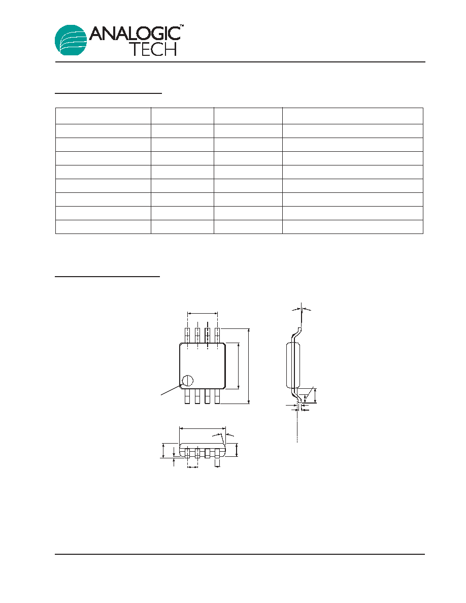
Package Information
MSOP8
PIN 1
1.95 BSC
0.254 BSC
0.155
±
0.075
0.60
±
0.20
3.00
±
0.10
0.95
±
0.15
0.95 REF
0.85
±
0.10
3.00
±
0.10
10
∞
±
5
∞
4
∞
±
4
∞
0.65 BSC
0.30
±
0.08
0.075
±
0.075
4.90
±
0.10
GAUGE PLANE
Output Voltage
Package
Marking
Part Number (Tape and Reel)
MSOP-8
4.1V
AAT3680IKS-4.1-T1
MSOP-8
4.2V
AAT3680IKS-4.2-T1
MSOP-8
8.2V
AAT3680IKS-8.2-T1
MSOP-8
8.4V
AAT3680IKS-8.4-T1
TSOPJW-12
4.1V
AAT3680ITP-4.1-T1
TSOPJW-12
4.2V
AAT3680ITP-4.2-T1
TSOPJW-12
8.2V
AAT3680ITP-8.2-T1
TSOPJW-12
8.4V
AAT3680ITP-8.4-T1
AAT3680
Lithium-Ion Linear Battery Charge Controller
3680.2003.4.0.91
17

TSOPJW-12
0.20 + 0.10
- 0.05
0.055
±
0.045
0.45
±
0.15
7
∞
NOM
4
∞ ±
4
∞
3.00
±
0.10
2.40
±
0.10
2.85
±
0.20
0.50 BSC 0.50 BSC 0.50 BSC 0.50 BSC 0.50 BSC
0.15
±
0.05
0.9625
±
0.0375
1.00
+ 0.10
-
0.065
0.04 REF
0.010
2.75
±
0.25
AAT3680
Lithium-Ion Linear Battery Charge Controller
18
3680.2003.4.0.91
Advanced Analogic Technologies, Inc.
830 E. Arques Avenue, Sunnyvale, CA 94085
Phone (408) 737-4600
Fax (408) 737-4611