AAT3682
Lithium-Ion/Polymer Linear Battery Charger
3682.2005.02.1.1
1
BatteryManager
TM
General Description
The AAT3682 is a lithium-ion/polymer linear battery
charger. It is designed for compact portable appli-
cations with a single cell battery. The AAT3682 pre-
cisely regulates battery charge voltage and charge
current, and offers an integrated pass device, mini-
mizing the number of external components required.
The AAT3682 charges the battery in three different
phases: preconditioning, constant current, and con-
stant voltage. In preconditioning mode, the charge
current has two different levels and is controlled by
one external pin. Battery charge temperature and
charge state are carefully monitored for fault condi-
tions. A battery charge stable monitor output pin is
provided to indicate the battery charge status
through a display LED or interface to a system con-
troller. The AAT3682 has the sleep mode option for
when the input supply is removed. In this mode, it
draws only 2.0µA of typical current.
The AAT3682 is available in a 16-pin QFN44 and is
specified over the -20∞C to +70∞C temperature
range.
Features
∑
V
IN
Range: 4.7V to 6.0V
∑
Low Quiescent Current, Typically 0.5mA
∑
1% Accurate Preset Voltage
∑
Up to 1A of Charging Current
∑
Integrated Pass Device
∑
Battery Temperature Monitoring
∑
Fast Trickle Charge Option
∑
Deep Discharge Cell Conditioning
∑
LED Charge Status Output or System
Microcontroller Serial Interface
∑
Power-On Reset
∑
Lower Power Sleep Mode
∑
Status Outputs for LED or System Interface
Indicates Charge and Fault Conditions
∑
Temperature Range: -20∞C to +70∞C
∑
16-Pin QFN44 Package
Applications
∑
Cellular Telephones
∑
Digital Still Cameras
∑
Hand-Held PCs
∑
MP3 Players
∑
Personal Data Assistants (PDAs)
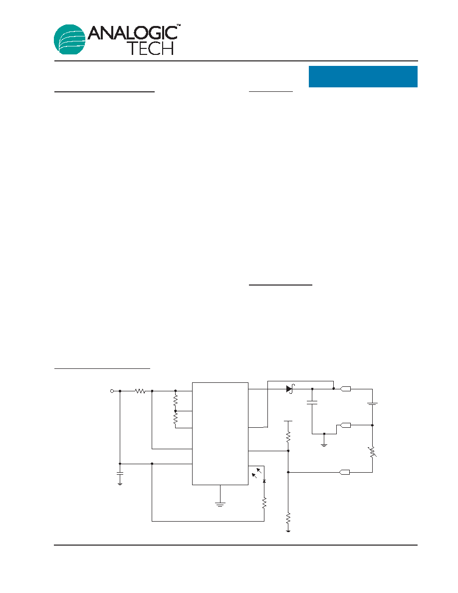
Typical Application
VP
Gate
DRV
CSI
VCC
VSS
BAT
T2X
BSENSE
TS
STAT
R
SENSE
C
IN
= 10
µ
F
C
OUT
= 1
µ
F
LED 1
R
2
= 1K
BATT+
BATT-
R
T1
VP
R
T2
TEMP
Adapter
R
4
R
3
Pin Description
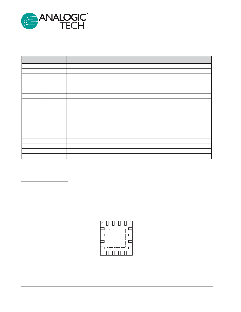
Pin Configuration
QFN44-16
(Top View)
1
2
3
4
12
11
10
9
5
6
7
8
16
15
14
13
TS
N/C
N/C
STAT
VSS
DR
V
T2X
N/C
BAT
VSS
GATE
N/C
AAT3682
VP
CSI
BSENSE
VCC
Pin #
Symbol
Function
1
TS
Battery temperature sense input.
2, 3, 8, 12
N/C
Not connected.
4
STAT
Battery charger status output. Connect an LED in series with 2.2k
from STAT to V
IN
for a visual monitor battery charge state or connect to a microcontroller to monitor bat-
tery status. A 100k
resistor should be placed between STAT and V
IN
for this function.
5
VSS
Common ground connection.
6
DRV
Battery charge control output.
7
T2X
Battery trickle charge control input. Connect this pin to V
SS
to double the battery trickle
charge current. Leave this pin floating for normal trickle current (10% of full charge cur-
rent). To enter microcontroller fast-read status, pull this pin high during power up.
9
BAT
Battery charge control output. Current regulated output to charge the battery. For best
operation, a 0.1µF ceramic capacitor should be placed between BAT and GND.
10
VSS
Common ground connection.
11
Gate
Input voltage for biasing the pass device.
13
VP
Battery charge power input.
14
CSI
Current sense input.
15
BSENSE
Battery voltage sense input.
16
VCC
AAT3682 bias input power.
EP
Exposed paddle (bottom); connect to GND directly beneath the package.
AAT3682
Lithium-Ion/Polymer Linear Battery Charger
2
3682.2005.02.1.1

Absolute Maximum Ratings
1
Thermal Information
Symbol
Description
Value
Units
JA
Maximum Thermal Resistance
2, 3
50
∞C/W
P
D
Power Dissipation (T
A
= 25∞C)
2.0
W
Symbol
Description
Value
Units
V
IN
V
IN
Relative to GND
-0.3 to 6.0
V
V
CSI
CSI to GND
-0.3 to V
CC
+0.3
V
V
T2X
T2X to GND
-0.3 to 5.5
V
Bias, V
BAT
BAT to GND
-0.3 to V
CC
+0.3
V
T
J
Operating Junction Temperature Range
-40 to 85
∞C
AAT3682
Lithium-Ion/Polymer Linear Battery Charger
3682.2005.02.1.1
3
1. Stresses above those listed in Absolute Maximum Ratings may cause permanent damage to the device. Functional operation at conditions
other than the operating conditions specified is not implied. Only one Absolute Maximum Rating should be applied at any one time.
2. Mounted on an FR4 board.
3. Derate 20mW/∞C above 25∞C.
Electrical Characteristics
1
V
IN
= 5.0V, T
A
= -20 to +70∞C, unless otherwise noted. Typical values are at T
A
= 25∞C.
Symbol
Description
Conditions
Min
Typ
Max Units
V
IN
Operation Input Voltage
4.7
6.0
V
I
CC
Operating Current
V
IN
= 5.5V, V
CH
= 4.2
0.5
3.0
mA
I
SLEEP
Sleep Mode Current
V
IN
= 3.5V, V
CH
= 4.2
3.0
6.0
µA
I
STAT(HI)
STAT High Level Output Leakage Current V
IN
= 5.5V
-1.0
+1.0
µA
V
STAT(LOW)
STAT Low Level Sink Current
V
IN
= 5.5V, I
SINK
= 5mA
0.3
0.6
V
V
CH
Output Charge Voltage Regulation
V
BAT
= 4.2V
T
A
= 25∞C
4.175
4.20
4.225
V
See Note 1
4.158
4.20
4.242
V
CS
Charge Current Regulation
V
IN
= 5.5V, V
CH
= 4.2
90
100
110
mV
I
CH
Charge Current
2
V
IN
= 5.5V
1.0
A
V
MIN
Preconditioning Voltage Threshold
V
CH
= 4.2V
3.04
3.1
3.16
V
V
TRICKLE
Trickle Charge Current Regulation
T2X Floating; V
CH
= 4.2V
10
mV
T
2X
Trickle Charge Current Gain
T2X = V
SS
1.8
V
TS1
Low Temperature Threshold
29.1
30
30.9
%V
CC
V
TS2
High Temperature Threshold
58.2
60
61.8
%V
CC
V
TERM
Charge Termination Threshold Voltage
4
12
24
mV
V
RCH
Battery Recharge Voltage Threshold
V
CH
= 4.2V
4.018
4.1
4.182
V
V
UVLO
Under-Voltage Lockout
V
IN
Rising, T
A
= 25∞C
3.5
4.0
4.5
V
V
OVP
Over-Voltage Protection Threshold
4.4
V
V
OCP
Over-Current Protection Threshold
200
%V
CS
AAT3682
Lithium-Ion/Polymer Linear Battery Charger
4
3682.2005.02.1.1
1. The AAT3682 output charge voltage is specified over 0∞C to 55∞C ambient temperature range; operation over -20∞C to 70∞C is guar-
anteed by design.
2. 1A of charging current is only for dynamic applications and not DC. In addition, the ambient temperature must be at or below 50∞C.
AAT3682
Lithium-Ion/Polymer Linear Battery Charger
3682.2005.02.1.1
5
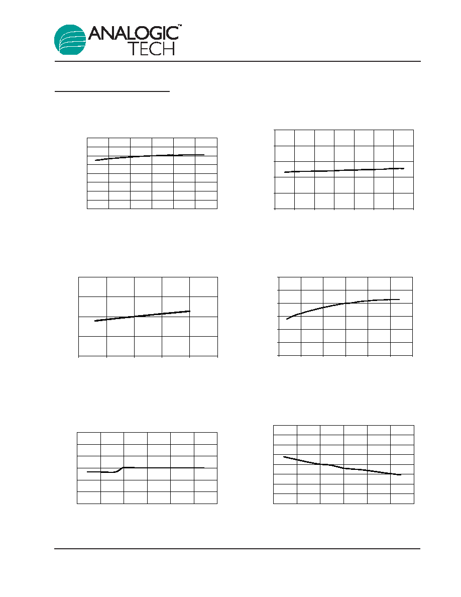
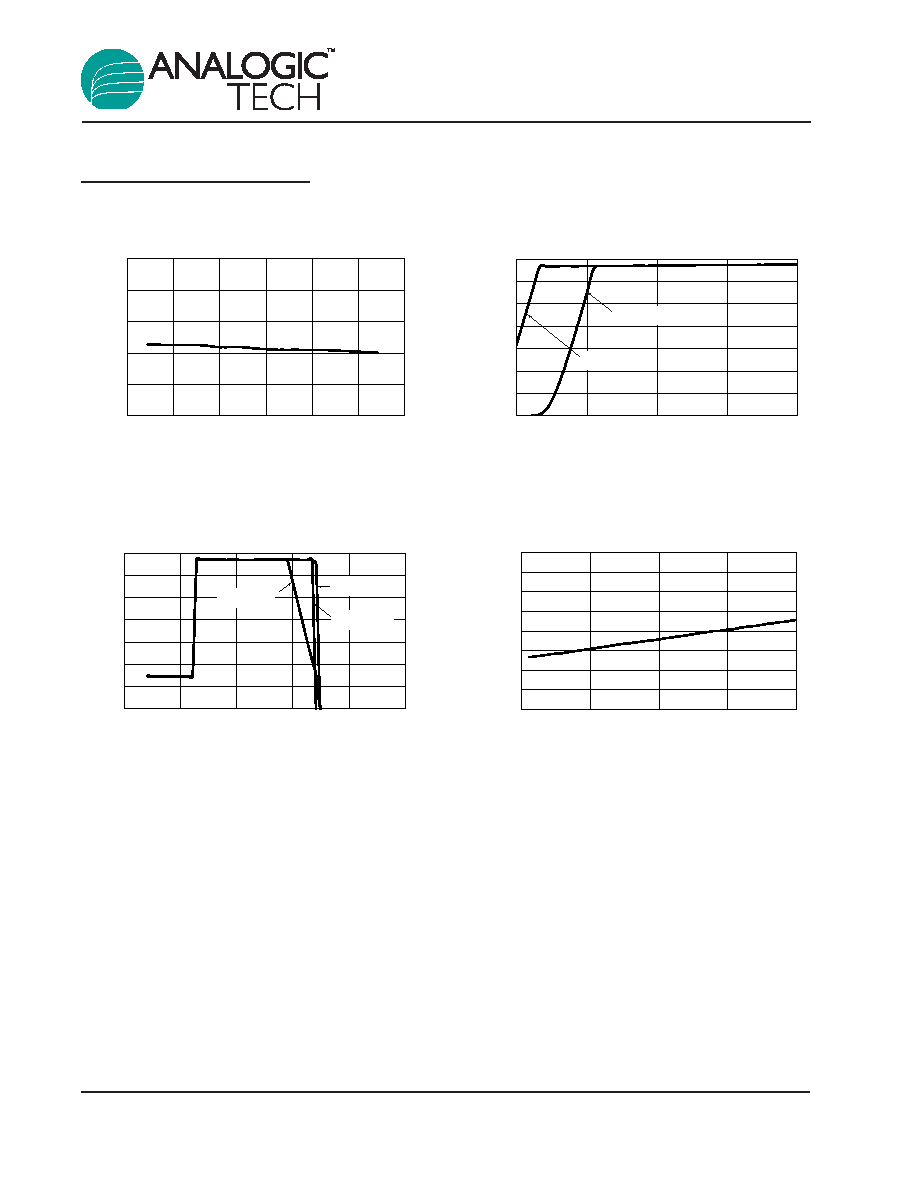
Typical Characteristics
Trickle Charge Current vs. Temperature
(R
SENSE
= 0.15
)
Temperature (
∞
C)
Trickle Charge Current
(mA)
130
135
140
145
150
155
160
165
170
-50
-25
0
25
50
75
100
Trickle Charge Threshold Voltage
vs.Temperature
(R
SENSE
= 0.15
)
Temperature (
∞
C)
Trickle Charge Threshold Voltage
(V)
2.8
2.9
3.0
3.1
3.2
3.3
3.4
-50
-25
0
25
50
75
100
Regulated Output Voltage vs. Temperature
(R
SENSE
= 0.15
)
Temperature (
∞
C)
Regulated Output Voltage
(V)
4.100
4.125
4.150
4.175
4.200
4.225
4.250
-50
-25
0
25
50
75
100
Regulated Output Voltage vs. Input Voltage
(R
SENSE
= 0.15
)
Input Voltage
(V)
Regulated Output Voltage
(V)
4.00
4.10
4.20
4.30
4.40
4.0
4.5
5.0
5.5
6.0
6.5
Regulated Output Voltage vs. Charge Current
(R
SENSE
= 0.15
)
Charging Current (mA)
Regulated Output Voltage (V)
4.15
4.17
4.19
4.21
4.23
4.25
0
100
200
300
400
500
600
700
Battery Recharge Threshold Voltage
vs.Temperature
(R
SENSE
= 0.15
)
Temperature (
∞
C)
Battery Recharge
Threshold Voltage
(V)
3.80
3.85
3.90
3.95
4.00
4.05
4.10
4.15
4.20
-50
-25
0
25
50
75
100
AAT3682
Lithium-Ion/Polymer Linear Battery Charger
6
3682.2005.02.1.1
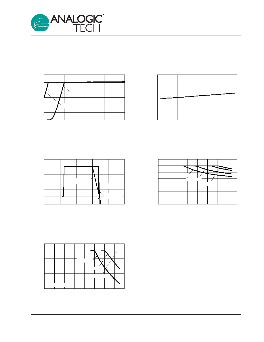
Typical Characteristics
Trickle Charge Current vs. Input Voltage
(R
SENSE
= 0.15
; 1.8X Mode)
Input Voltage (V)
Trickle Charge Current
(mA)
130
135
140
145
150
155
160
165
170
4.0
4.5
5.0
5.5
6.0
Charging Current vs. Battery Voltage
(R
SENSE
= 0.15
with External Schottky)
Battery Voltage (V)
Charging Current
(mA)
0
100
200
300
400
500
600
700
2.5
3.0
3.5
4.0
4.5
5.0
V
IN
= 4.5V
V
IN
= 4.75V
V
IN
= 5.5V
Charging Current vs. Input Voltage
(R
SENSE
= 0.15
with External Schottky)
Input Voltage (V)
Charging Current
(mA)
0
100
200
300
400
500
600
700
4.0
4.5
5.0
5.5
6.0
V
BAT
= 4.1V
V
BAT
= 3.6V
Charging Current vs. Temperature
(R
SENSE
= 0.15
)
Temperature (
∞
C)
Charging Current
(mA)
650
660
670
680
690
700
-50
-25
0
25
50
75
100
Typical Characteristics
Safe Operating Area
(T
J(MAX)
= 150
∞
C)
Charging Current (A)
Maximum Input Voltage (V)
5.0
5.2
5.4
5.6
5.8
6.0
6.2
0
0.2
0.4
0.6
0.8
T
AMB
= 85
∞
C
T
AMB
= 70
∞
C
T
AMB
= <50
∞
C
Schottky V
F
= 0.2V
Safe Operating Area
(T
J(MAX)
= 120
∞
C)
Charging Current (A)
Maximum Input Voltage (V)
0.0
1.0
2.0
3.0
4.0
5.0
6.0
7.0
0.0
0.2
0.4
0.6
0.8
T
AMB
= 85
∞
C
Schottky V
F
= 0.2V
T
AMB
= 70
∞
C
T
AMB
= 50
∞
C
T
AMB
= 40
∞
C
Charging Current vs. Battery Voltage
(R
SENSE
= 0.2
with External Schottky)
Battery Voltage (V)
Charging Current
(mA)
0
100
200
300
400
500
600
2.5
3.0
3.5
4.0
4.5
5.0
V
IN
= 4.5V
V
IN
= 4.75V
V
IN
= 5.5V
Trickle Charge Current vs. Input Voltage
(R
SENSE
= 0.2
; 1.8X Mode)
Input Voltage (V)
Trickle Charge Current
(mA)
94
96
98
100
102
104
4
4.5
5
5.5
6
Charging Current vs. Input Voltage
(R
SENSE
= 0.2
with External Schottky)
Input Voltage (V)
Charging Current
(mA)
0
100
200
300
400
500
600
4.0
4.5
5.0
5.5
6.0
V
BAT
= 4.0V
V
BAT
= 3.6V
AAT3682
Lithium-Ion/Polymer Linear Battery Charger
3682.2005.02.1.1
7
AAT3682
Lithium-Ion/Polymer Linear Battery Charger
8
3682.2005.02.1.1
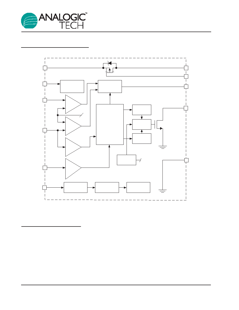
Functional Block Diagram
MUX
T2X
LED Signal
Generator
Microcontroller
Status Generator
Microcontroller
Read Enable
Charge Status
Logic Control
Power-On
Reset
V
SS
STAT
DRV
GATE
BAT
Under-Voltage
Lock Out
Over-Current /
Short-Circuit
Protection
2X Trickle
Charge
Control
Loop Select
MUX
Driver
V
REF
Temperature
Sense
Comparator
Voltage
Comparator
Voltage Loop
Error Amp
Current Loop
Error Amp
V
P
V
CC
B
SENSE
T2X
TS
CSI
Functional Description
The AAT3682 is a linear charger designed for single
cell lithium-ion/polymer batteries. It is a full-featured
battery management system IC with multiple levels
of power savings, system communication, and pro-
tection integrated inside. Refer to the block diagram
above and the flow chart and typical charge profile
graph (Figures 1 and 2) in this section.
Cell Preconditioning
Before the start of charging, the AAT3682 checks
several conditions in order to maintain a safe charg-
ing environment. The input supply must be above
the minimum operating voltage, or under-voltage
lockout threshold (V
UVLO
), for the charging
sequence to begin. Also, the cell temperature, as
reported by a thermistor connected to the T
S
pin,
must be within the proper window for safe charging.

AAT3682
Lithium-Ion/Polymer Linear Battery Charger
3682.2005.02.1.1
9
Figure 1: AAT3682 Operational Flow Chart.
Figure 2: Typical Charge Profile.
Preconditioning
(Trickle Charge)
Phase
Constant Current
Phase
Constant Voltage
Phase
Output Charge
Voltage (V
CH
)
Preconditioning
Voltage Threshold
(V
MIN
)
Regulation
Current
(I
CHARGE(REG)
)
Trickle Charge
and Termination
Threshold
UVLO
Temperature Test
TS > V
TS1
TS < V
TS2
Power On Reset
Power On Reset
Preconditioning Test
Current Phase Test
V
CH
> V
BAT
V
MIN
> V
BAT
V
TERM
R
SENSE
< V
RCH
Voltage
Phase Test
V
CC
> V
UVLO
Shut Down
Mode
Shut Down
Mode
Yes
No
Yes
Yes
Low Current
Conditioning
Charge
Low Current
Conditioning
Charge
(Trickle Charge)
Temperature
Fault
Temperature
Fault
No
No
Current
Charging
Mode
Current
Charging
Mode
Yes
Voltage
Charging
Mode
Voltage
Charging
Mode
< I
BAT
No
Yes
No
Charge Complete
Latch Off
Charge Complete
Latch Off

AAT3682
Lithium-Ion/Polymer Linear Battery Charger
10
3682.2005.02.1.1
When these conditions have been met and a bat-
tery is connected to the BAT pin, the AAT3682
checks the state of the battery. If the cell voltage is
below V
MIN
, the AAT3682 begins preconditioning
the cell. This is performed by charging the cell with
10% of the programmed constant-current amount.
For example, if the programmed charge current is
500mA, then the preconditioning mode (trickle
charge) current will be 50mA. Cell preconditioning
is a safety precaution for deeply discharged cells
and, furthermore, limits power dissipation in the
pass transistor when the voltage across the device
is largest. The AAT3682 features an optional T2X
mode, which allows faster trickle-charging at
approximately two times the default rate. This
mode is selected by connecting the T2X pin to V
SS
.
If an over-temperature fault is triggered, the fast
trickle-charge will be latched off, and the AAT3682
will continue at the default 10% charge current.
Constant Current Charging
The cell preconditioning continues until the voltage
on the BAT pin reaches V
MIN
. At this point, the
AAT3682 begins constant-current charging (fast
charging). Current level for this mode is pro-
grammed using a current sense resistor R
SENSE
between the V
CC
and CSI pins. The CSI pin moni-
tors the voltage across R
SENSE
to provide feedback
for the current control loop. The AAT3682 remains
in constant current charge mode until the battery
reaches the voltage regulation point, V
CH
.
Constant Voltage Charging
When the battery voltage reaches V
CH
during con-
stant-current mode, the AAT3682 transitions to con-
stant-voltage mode. The regulation voltage is facto-
ry programmed to 4.2V. In constant-voltage opera-
tion, the AAT3682 monitors the cell voltage and ter-
minates the charging cycle when the voltage across
R
SENSE
decreases to approximately 10mV.
Charge Cycle Termination, Recharge
Sequence
After the charge cycle is complete, the AAT3682
shuts off the pass device and automatically enters
power-saving sleep mode. Either of two possible
conditions will bring the IC out of sleep mode: the
battery voltage at the BAT pin drops below V
RCH
(recharge threshold voltage) or the AAT3682 is
reset by cycling the input supply through the
power-on sequence. Falling below V
RCH
signals the
IC that it is time to initiate a new charge cycle.
Sleep Mode
When the input supply is disconnected, the device
automatically enters power-saving sleep mode. Only
consuming an ultra-low 2µA current, the AAT3682
minimizes battery drain when it is not charging. This
feature is particularly useful in applications where
the input supply level may fall below the battery
charge or under-voltage lockout level. In such cases,
where the AAT3682 input voltage drops, the device
will enter the sleep mode and automatically resume
charging once the input supply has recovered from
its fault condition. This makes the AAT3682 well suit-
ed for USB battery charger applications.
Charge Inhibit
The AAT3682 charging cycle is fully automatic;
however, it is possible to stop the device from
charging even when all conditions are met for prop-
er charging. Switching the T
S
pin to either V
IN
or
GND will force the AAT3682 to turn off the pass
device and wait for a voltage between the low and
high temperature voltage thresholds.
Resuming Charge and the V
RCH
Threshold
The AAT3682 will automatically resume charging
under most conditions when a battery charge cycle
is interrupted. Events such as an input supply
interruption or under voltage, removal and replace-
ment of the battery under charge, or charging a
partially drained battery are all possible. The
AAT3682 will monitor the battery voltage and auto-
matically resume charging in the appropriate mode
based upon the measured battery cell voltage.
This feature is useful for systems with an unstable
input supply, which could be the case when power-
ing a charger from a USB bus supply. It is also
beneficial for charging or "topping off" partially dis-
charged batteries. The only restriction on resum-
ing charge of a battery is that the battery cell volt-
age must be below the battery recharge voltage
threshold (V
RCH
) specification. There is V
RCH
threshold hysteresis built into the charge control

system. This is done to prevent the charger from
erroneously turning on and off once a battery
charge cycle is complete.
For example, the AAT3682 has a typical V
RCH
threshold of 4.1V. A battery under charge is above
4.1V, but is still in the constant voltage mode
because it has not yet reached 4.2V to complete
the charge cycle. If the battery is removed and
then placed back on the charger, the charge cycle
will not resume until the battery voltage drops
below the V
RCH
threshold. In another case, a bat-
tery under charge is in the constant current mode
and the cell voltage is 3.7V when the input supply
is inadvertently removed and then restored. The
battery is below the V
RCH
threshold and the charge
cycle will immediately resume where it left off.
LED Display Charge Status Output
The AAT3682 provides a battery charge status out-
put via the STAT pin. STAT is an open-drain serial
data output capable of displaying five distinct status
functions with one LED connected between the
STAT pin and V
P
. There are four periods which
determine a status word. Under default conditions,
each output period is one second long; thus one
status word will take four seconds to display
through an LED. The five modes include:
1. Sleep/Charge Complete: The IC goes into
Sleep mode when no battery is present -OR-
when the charge cycle is complete.
2. Fault: When an Over-Current (OC) condition
is detected by the current sense and control
circuit -OR- when an Over-Voltage (OV) con-
dition is detected at the BAT pin -OR- when a
battery Over-Temperature fault is detected
on the TEMP pin.
3. Battery Conditioning: When the charge sys-
tem is in the 1X or 2X trickle charge mode.
4. Constant Current (CC) Mode: When the sys-
tem is in the constant current charge mode.
5. Constant Voltage (CV) Mode: When the sys-
tem is in the constant voltage charge mode.
An additional feature of the LED status display is for
a Battery Not Detected state. When the AAT3682
senses there is no battery connected to the BAT
pin, the STAT output will turn the LED on and off at
a rate dependent on the size of the output capacitor
being used. The LED cycles on for two periods then
remains off for two periods. See Figure 3 below.
AAT3682
Lithium-Ion/Polymer Linear Battery Charger
3682.2005.02.1.1
11
Figure 3: LED Display Output.
Sleep / Charge Complete
Temp., OC, OV Fault
Battery Conditioning
Constant Current Mode
Constant Voltage Mode
off / off / off / off
on / on / off / off
on / on / on / on
on / off / off / off
on / on / on / off
Charge Status
Output Status
LED Display
on/off
ON
OFF
ON
OFF
ON
OFF
ON
OFF
ON
OFF
on/off
on/off
on/off
AAT3682
Lithium-Ion/Polymer Linear Battery Charger
12
3682.2005.02.1.1
High-Speed Data Reporting
An optional system microcontroller interface can be
enabled by pulling the T2X pin up to 4.5V to 5.5V
during power-up sequence. The T2X pin should be
pulled high with the use of a 100k
resistor. If the
input supply to V
IN
will not exceed 5.5V, then the
T2X pin may be tied directly to V
IN
through a
100K
resistor. Since this is a TTL level circuit, it
may not be pulled higher than 5.5V without risk of
damage to the device.
When the high-speed data report feature is
enabled, the STAT output periods are sped up to
40µs, making the total status word 160µs in length.
See Figure 4 below.
An additional feature is the Output Status for the
Battery Not Detected state. When the AAT3682
senses there is no battery connected to the BAT
pin, the STAT pin cycles for two periods, then
remains off for two periods. When in High-Speed
Data Reporting, the AAT3682 will only trickle
charge at the 2X trickle charge level. This is
because the T2X pin is pulled high to enable the
high-speed data reporting. A status display LED
may not be connected to the STAT pin when the
high-speed data reporting is being utilized. If both
display modes are required, the display LED must
be switched out of the circuit before the T2X pin is
pulled high. Failing to do so could cause problems
with the high-speed switching control circuits inter-
nal to the AAT3682.
Charge Complete LED Status Mode
A simplified LED status can be obtained by config-
uring the AAT3682 for high-speed data recording
mode (T2X tied to V
CC
) and installing a 0.047µF
capacitor from the STAT pin to the V
SS
pin (see
Figure 5). In this configuration, the LED will be illu-
minated for all modes except the Sleep/Charge
Complete mode. In addition, the T2X input must be
tied to V
CC
through a 100k
resistor. In this mode,
the trickle charge current will be 1.8X the normal
trickle charge level. To reset the trickle charge cur-
rent to the 1X level, the T
S
input must be temporar-
ily toggled low. Removing C3 forces the LED status
to gradually dim out as the battery becomes fully
charged (see Figure 5).
Figure 4: Microcontroller Interface Logic Output.
Sleep / Charge Complete
Temp., OC, OV Fault
Battery Conditioning
Constant Current Mode
Constant Voltage Mode
HI / HI / HI / HI
LO / LO / HI / HI
LO / LO / LO / LO
LO / HI / HI / HI
LO / LO / LO / HI
Charge Status
Output Status
STAT Level

Protection Circuitry
The AAT3682 is a highly integrated battery manage-
ment system IC including several protection fea-
tures. In addition to battery temperature monitoring,
the IC constantly monitors for over-current and over-
voltage conditions; if an over-current situation
occurs, the AAT3682 latches off the pass device to
prevent damage to the battery or the system, and
enters shutdown mode until the over-current event is
terminated. An over-voltage condition is defined as a
condition where the voltage on the BAT pin exceeds
the maximum battery charge voltage. If an over-volt-
age condition occurs, the IC turns off the pass
device until voltage on the BAT pin drops below the
maximum battery charge constant voltage threshold.
The AAT3682 will resume normal operation after the
over-current or over-voltage condition is removed.
During an over-current or over-voltage event, the
STAT will report a FAULT signal. In the event of a
battery over-temperature condition, the IC will turn
off the pass device and report a FAULT signal on the
STAT pin. After the system recovers from a temper-
ature fault, the IC will resume operation in the 1X
trickle charge mode to prevent damage to the sys-
tem in the event a defective battery is placed under
charge. Once the battery voltage rises above the
trickle charge to constant current charge threshold,
the IC will resume the constant current mode.
Applications Information
Choosing a Sense Resistor
The charging rate recommended by Lithium-Ion
cell vendors is normally 1C, with a 2C absolute
maximum rating. Charging at the highest recom-
mended rate offers the advantage of shortened
charging time without decreasing the battery's lifes-
pan. This means that the suggested fast charge
rate for a 500mAH battery pack is 500mA. Refer to
the Safe Operating Area curves in the Typical
Characteristics section of this datasheet to deter-
mine the maximum allowable charge current for a
given input voltage. The current sense resistor,
R
SENSE
, programs the charge current according to
the following equation:
Where I
CHARGE
is the desired typical charge current
during constant-current charge mode. V
CC
- V
CSI
is
the voltage across R
SENSE
, shown in the Electrical
Characteristic table as V
CS
. To program a nominal
500mA charge current during fast-charge, a
200m
value resistor should be selected.
V
CC
- V
CSI
R
SENSE
=
I
CHARGE
AAT3682
Lithium-Ion/Polymer Linear Battery Charger
3682.2005.02.1.1
13
Figure 5: Evaluation Board Schematic.
1
2
J1
1
2
3
J2
1K
R4
0.2
R2
1K
R3
2.2K
R1
100K
R6
100K
R5
D2
22
µ
F
C1
10
µ
F
C2
Green LED
V
IN
GND
D1
47nF
C3
TS
1
N/C
2
N/C
3
STAT
4
VSS
5
DRV
6
T2X
7
N/C
8
BAT
9
VSS
10
Gate
11
N/C
12
VP
13
CSI
14
BSENSE
15
VCC
16
AAT3682
U1
100K
R7
2
1
3
SW-T2X
S1
1000pF
C4
4.7
µ
F
C5
Remove capacitor for
progressive dimming

AAT3682
Lithium-Ion/Polymer Linear Battery Charger
14
3682.2005.02.1.1
Calculate the worst case power dissipated in the
sense resistor according to the following equation:
A 500mW LRC type sense resistor from IRC is
adequate for this purpose. Higher value sense
resistors can be used, decreasing the power dissi-
pated in the sense resistor and pass transistor.
The drawback of higher value sense resistors is
that the charge cycle time is increased, so tradeoffs
should be considered when optimizing the design.
Thermistor
The AAT3682 checks battery temperature before
starting the charge cycle, as well as during all stages
of charging. This is accomplished by monitoring the
voltage at the T
S
pin. Either a negative temperature
coefficient thermistor (NTC) or positive-temperature
coefficient thermistor (PTC) can be used because
the AAT3682 checks to see that the voltage at T
S
is
within a voltage window bounded by V
TS1
and V
TS2
.
Please see the following equations for specifying
resistors:
R
T1
and R
T2
for use with NTC Thermistor
R
T1
and R
T2
for use with PTC Thermistor
Where R
TC
is the thermistor's cold temperature
resistance and R
TH
is the thermistor's hot tempera-
ture resistance. See thermistor specifications for
additional information. To ensure there is no
dependence on the input supply changes, connect
divider between V
CC
and V
SS
. Disabling the tem-
perature-monitoring function is achieved by apply-
ing a voltage between V
TS1
and V
TS2
on the T
S
pin.
Capacitor Selection
Input Capacitor
In general, it is good design practice to place a
decoupling capacitor between the V
CC
and V
SS
pins. An input capacitor in the range of 1µF to 10µF
is recommended. If the source supply is unregu-
lated, it may be necessary to increase the capaci-
tance to keep the input voltage above the under-
voltage lockout threshold. If the AAT3682 is to be
used in a system with an external power supply
source, such as a typical AC-to-DC wall adaptor,
then a C
IN
capacitor in the range of 10µF should be
used. A larger input capacitor in this application will
minimize switching or power bounce effects when
the power supply is "hot plugged" in.
Output Capacitor
The AAT3682 does not need an output capacitor for
stability of the device itself. However, a capacitor
connected between BAT and V
SS
will control the
output voltage when the AAT3682 is powered up
when no battery is connected. The AAT3682 can
become unstable if a high impedance load is placed
across the BAT pin to V
SS
. Such a case is possible
with aging Li-Ion battery cells. As cells age through
repeated charge and discharge cycles, the internal
impedance can rise over time. A 10µF or larger out-
put capacitor will compensate for the adverse
effects of a high impedance load and assure device
stability over all operating conditions.
Power Dissipation
The voltage drop across the V
P
and BAT pins mul-
tiplied times the charge current is used to deter-
mine the internal power dissipation. The maximum
power dissipation occurs when the input voltage is
at a maximum and the battery voltage is at the min-
imum preconditioning voltage threshold. This
power is then multiplied times the package theta to
determine the maximum junction temperature. The
worst case power junction temperature is calculat-
ed as follows.
R
T1
=
5 ∑ R
TH
∑
R
TC
3 ∑ (R
TC
-
R
TH
)
R
T2
=
5 ∑ R
TH
∑
R
TC
(2 ∑ R
TH
) - (7 ∑ R
TC
)
R
T1
=
5 ∑ R
TH
∑
R
TC
3 ∑ (R
TC
-
R
TH
)
R
T2
=
5 ∑ R
TH
∑
R
TC
(2 ∑ R
TC
) - (7 ∑ R
TH
)
V
CS
2
0.1V
2
P = = = 50mW
R
SENSE
0.2
AAT3682
Lithium-Ion/Polymer Linear Battery Charger
3682.2005.02.1.1
15
This equation can be used to determine the maxi-
mum input voltage given the maximum junction and
ambient temperature and desired charge current.
Operation Under No-Load
Under no-load conditions (i.e., when the AAT3682 is
powered with no battery connected between the
BAT pin and V
SS
), the output capacitor is charged up
very quickly by the trickle charge control circuit to the
BAT pin until the output reaches the recharge
threshold (V
RCH
). At this point, the AAT3682 will
drop into sleep mode. The output capacitor will dis-
charge slowly by the capacitor's own internal leak-
age until the voltage seen at the BAT pin drops
below the V
RCH
threshold. This 100mV cycle will
continue at approximately 3Hz with a 0.1µF capaci-
tor connected. A larger capacitor value will produce
a slower voltage cycle. This operation mode can be
observed by viewing the STAT LED blinking on and
off at the rate established by the C
OUT
value. For
desktop charger applications, where it might not be
desirable to have a "charger ready" blinking LED, a
large C
OUT
capacitor in the range of 100µF or more
would prevent the operation of this mode.
AAT3682 features charge status output. Connecting
a LED to the STAT pin will display all the three con-
ditions of battery operation. Once the adapter is
connected to the battery charger, the LED will be
fully illuminated. As the battery charges, the LED
will gradually dim as it transitions to constant current
mode and to constant voltage mode. Table 1 sum-
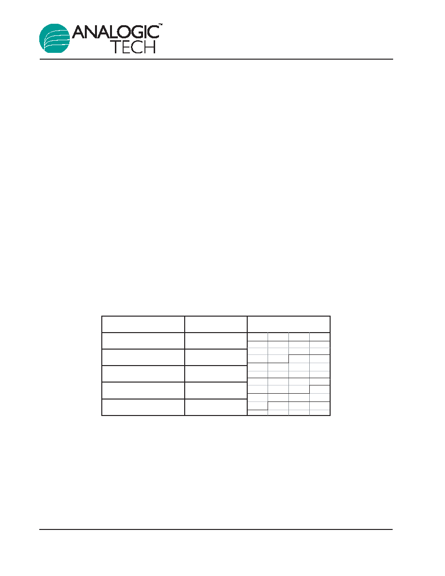
marizes the conditions.
Table 1: Charging Status.
For applications where gradual dimming of the LED
is not desired, adding C3 (refer to Figure 5) between
the STAT pin and VSS will alter the charging status.
In addition, the AAT3682 must be configured to
operate in the high frequency STAT mode by con-
necting the T2X pin to VCC via 100K
resistor.
As the battery is transitioning from trickle charge to
constant current charge and constant voltage, the
LED will remain illuminated. Once the battery is fully
charged, the LED will shut off indicating completion
of charge. Table 2 summarizes the conditions.
Table 2: Charging Status With C3 Connected.
Reverse Current Blocking Diode
A reverse-blocking diode is generally required for
the circuit shown in Figure 5.
The blocking diode gives the system protection from
a shorted input. If there is no other protection in the
system, a shorted input could discharge the battery
through the body diode of the internal pass MOS-
FET. If a reverse-blocking diode is added to the sys-
tem, a device should be chosen that can withstand
the maximum constant-current charge current at the
maximum system ambient temperature.
Additionally, the blocking diode will prevent the bat-
tery from being discharged to the UVLO level by
the AAT3682 in the event that power is removed
from the input to the AAT3682. For this reason, the
blocking diode must be placed in the location
shown in Figure 5.
Charge Status
LED Display
No battery connected
Blinking
Battery condition
On
cc
On
cv
On
Sleep/charge complete
Off
Charge Status
LED Display
No battery connected
blinking
Battery condition
100% LED light
cc
75% LED light
cv
25% LED light
Sleep/charge complete
off
T
J(MAX)
- T
AMB
V
IN(MAX)
= + V
BAT
+ V
SCHOTTKY
+ V
CS
= + 3.1V + 0.2V + 0.1V
= 5.3V
I
CHG(MAX)
120
∞
C - 70
∞
C
50
∞
C/W
500mA
P
MAX
= (V
IN(MAX)
- V
SENSE
- V
SCHOTTKY
- V
BAT(MIN)
)
I
CHG(MAX)
= (5.5V - 0.1V - 0.2V - 3.04V)
550mA
= 1.2W

AAT3682
Lithium-Ion/Polymer Linear Battery Charger
16
3682.2005.02.1.1
Diode Selection
Typically, a Schottky diode is used in reverse cur-
rent blocking applications with the AAT3682. Other
lower cost rectifier type diodes may also be used to
save cost if sufficient input power supply head
room is available.
The blocking diode selection should based on merits
of the device forward voltage (V
F
), current rating,
input supply level versus the maximum battery
charge voltage, and cost.
First, one must determine the appropriate minimum
diode forward voltage drop. Refer to the following
equation:
V
IN(MIN)
= V
BAT(MAX)
+ V
F(TRAN)
+ V
F(DIODE)
Where:
V
IN(MIN)
= Minimum input supply level
V
BAT(MAX)
= Maximum battery charge voltage required
V
F(TRAN)
= Pass transistor forward voltage drop
V
F(DIODE)
= Blocking diode forward voltage
Based on the maximum constant current charge
level set for the system, the next step is to determine
the minimum current rating and power handling
capacity for the blocking diode. The constant current
charge level itself will dictate what the minimum cur-
rent rating must be for a given blocking diode. The
minimum power handling capacity must be calculat-
ed based on the constant current amplitude and the
diode forward voltage (V
F
):
Where:
P
D(MIN)
= Minimum power rating for a diode selection
V
F
= Diode forward voltage
I
CC
= Constant current charge level for the system
Schottky Diodes
Schottky diodes are selected for this application
because they have a low forward voltage drop, typi-
cally between 0.3V and 0.4V. A lower V
F
permits a
lower voltage drop at the constant current charge
level set by the system; less power will be dissipated
in this element of the circuit. A Schottky diode allows
for lower power dissipation, smaller component
package sizes, and greater circuit layout densities.
Rectifier Diodes
Any general purpose rectifier diode can be used with
the AAT3682 application circuit in place of a higher
cost Schottky diode. The design trade-off is that a
rectifier diode has a high forward voltage drop. V
F
for a typical silicon rectifier diode is in the range of
0.7V. A higher V
F
will place an input supply voltage
requirement for the battery charger system. This will
also require a higher power rated diode since the
voltage drop at the constant current charge ampli-
tude will be greater. Refer to the previously stated
equations to calculate the minimum V
IN
and diode
P
D
for a given application.
V
F
P
D(MIN)
=
I
CC

AAT3682
Lithium-Ion/Polymer Linear Battery Charger
3682.2005.02.1.1
17
Figure 6: Evaluation Board Top Side Layout.
Figure 7: Evaluation Board Bottom Side Layout.
Reference
Component
Designator
Description
Footprint
Part Number
Manufacturer
U1
Battery Charger AAT3682
QFN44-16
AAT3682-4.2
AnalogicTech
C1
Ceramic Capacitor 20µF-10V-X5R
1210
GRM32ER61A226KA65L muRata
C2
Ceramic Capacitor 10µF-10V-X5R
0805
GRM21BR61A106KE19L muRata
C3
Ceramic Capacitor 0.047µF-10V-X7R
0805
VJ0805Y473KXQA
Vishay
R1
Resistor 2.2K
1/4W
0402
CRCW04022211F
Vishay
R2
Current Sensing Resistor 0.2
1/4W
0805
RL1220S-R20-F
SSM Susumu
R3
Resistor 1.0K
1% 1/4W
0402
CRCW04021003F
Vishay
R4
Resistor 1.0K
1% 1/4W
0402
CRCW04021001F
Vishay
R5
Resistor 100K
1% 1/4W
0402
CRCW04021003F
Vishay
R6
Resistor 100K
1% 1/4W
0402
CRCW04021003F
Vishay
R7
Resistor 100K
1% 1/4W
0402
CRCW04021003F
Vishay
J1
4-Pin Socket Connector
4 Pin
277-1273-ND
J2
6-Pin Socket Connector
6 Pin
277-1274-ND
S1
Jumper Stand Switch
2 mm Jumper S2105-40-ND
D1
Green LED
1206
L62215CT-ND
Chicago Miniature
D2
3.0A Schottky Diode
SMA
B340LADITR-ND
Diodes Incorporated
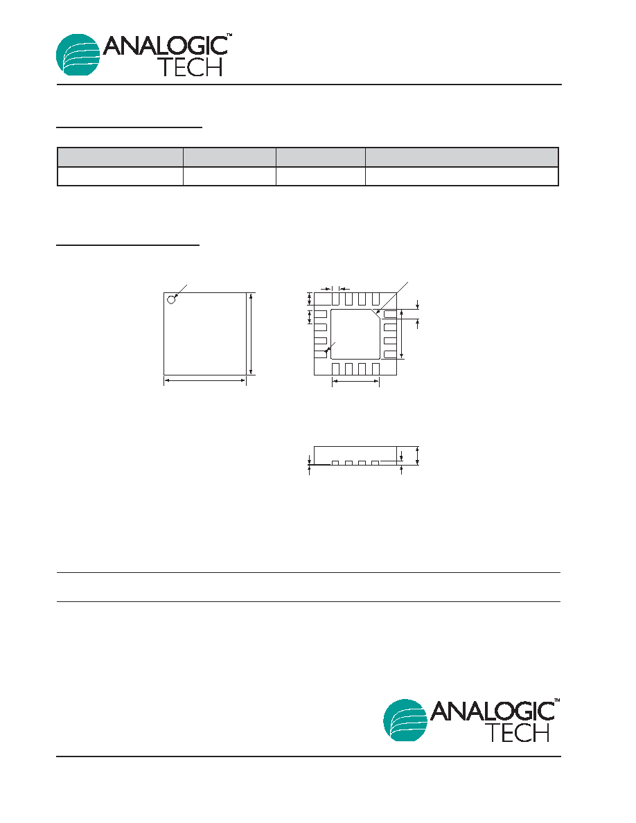
Ordering Information
Package Information
All dimensions in millimeters.
4.000
±
0.050
Pin 1 Dot By Marking
2.400
±
0.050
0.600
±
0.050
4.000
±
0.050
2.280 REF
0.650 BSC
0.900
±
0.050
Pin 1 Identification
R0.030Max
1
4
5
8
9
13
16
0.450
±
0.050
0.0125
±
0.0125
0.203
±
0.025
0.330
±
0.050
Top View
Bottom View
Side View
Output Voltage
Package
Marking
1
Part Number (Tape and Reel)
2
4.2V
QFN44-16
MGXXY
AAT3682ISN-4.2-T1
AAT3682
Lithium-Ion/Polymer Linear Battery Charger
18
3682.2005.02.1.1
Advanced Analogic Technologies, Inc.
830 E. Arques Avenue, Sunnyvale, CA 94085
Phone (408) 737-4600
Fax (408) 737-4611
AnalogicTech cannot assume responsibility for use of any circuitry other than circuitry entirely embodied in an AnalogicTech product. No circuit patent licenses, copyrights, mask work
rights, or other intellectual property rights are implied.
AnalogicTech reserves the right to make changes to their products or specifications or to discontinue any product or service without notice, and advise customers to obtain the latest
version of relevant information to verify, before placing orders, that information being relied on is current and complete. All products are sold subject to the terms and conditions of sale
supplied at the time of order acknowledgement, including those pertaining to warranty, patent infringement, and limitation of liability.
AnalogicTech warrants performance of its semiconductor products to the specifications applicable at the time of sale in accordance with AnalogicTech's standard warranty. Testing and
other quality control techniques are utilized to the extent AnalogicTech deems necessary to support this warranty. Specific testing of all parameters of each device is not necessarily
performed.
1. XYY = assembly and date code.
2. Sample stock is generally held on part numbers listed in BOLD.