SmartSwitch
TM
AAT4601A
1.8A Current Limited P-Channel Switch
4601A.2006.05.1.5
1
General Description
The AAT4601A SmartSwitch is a member of
AnalogicTech's Application Specific Power
MOSFETTM (ASPMTM) product family. It is a 1.8A
current limited P-channel MOSFET power switch
designed for high-side load switching applications.
This switch operates with inputs ranging from 2.7V
to 5.5V, making it ideal for both 3V and 5V systems.
An integrated current-limiting circuit protects the
input supply against large changes in load current
which could cause the supply to fall out of regula-
tion. The AAT4601A has protection from thermal
overload which limits power dissipation and junction
temperatures. The maximum current limit level will
guarantee that 1.8A can be delivered to the load;
the actual threshold is programmed with a resistor
from the SET pin to ground. The quiescent supply
current is typically 12ĶA. In shutdown mode, the
supply current decreases to less than 1ĶA.
The AAT4601A is available in a Pb-free, 8-pin SOP,
TSSOP, or MSOP package and is specified over
the -40įC to +85įC temperature range.
Features
∑
Input Voltage: 2.7V to 5.5V
∑
Programmable Over-Current Threshold
∑
Low Quiescent Current
-- 12ĶA Typical
-- Less Than 1ĶA with Switch Off
∑
Only 2.5V Needed for ON Control
∑
Thermal Shutdown
∑
Fault Flag
∑
2ms Fault Blanking
∑
Under-Voltage Lockout
∑
Temperature Range: -40įC to +85įC
∑
4kV ESD rating
∑
UL Approved--File No. E217765
∑
8-Pin SOP, TSSOP, or MSOP Package
Applications
∑
Hot Swap Supplies
∑
Notebook Computers
∑
Peripheral Ports
∑
USB Ports
UL Recognized Component
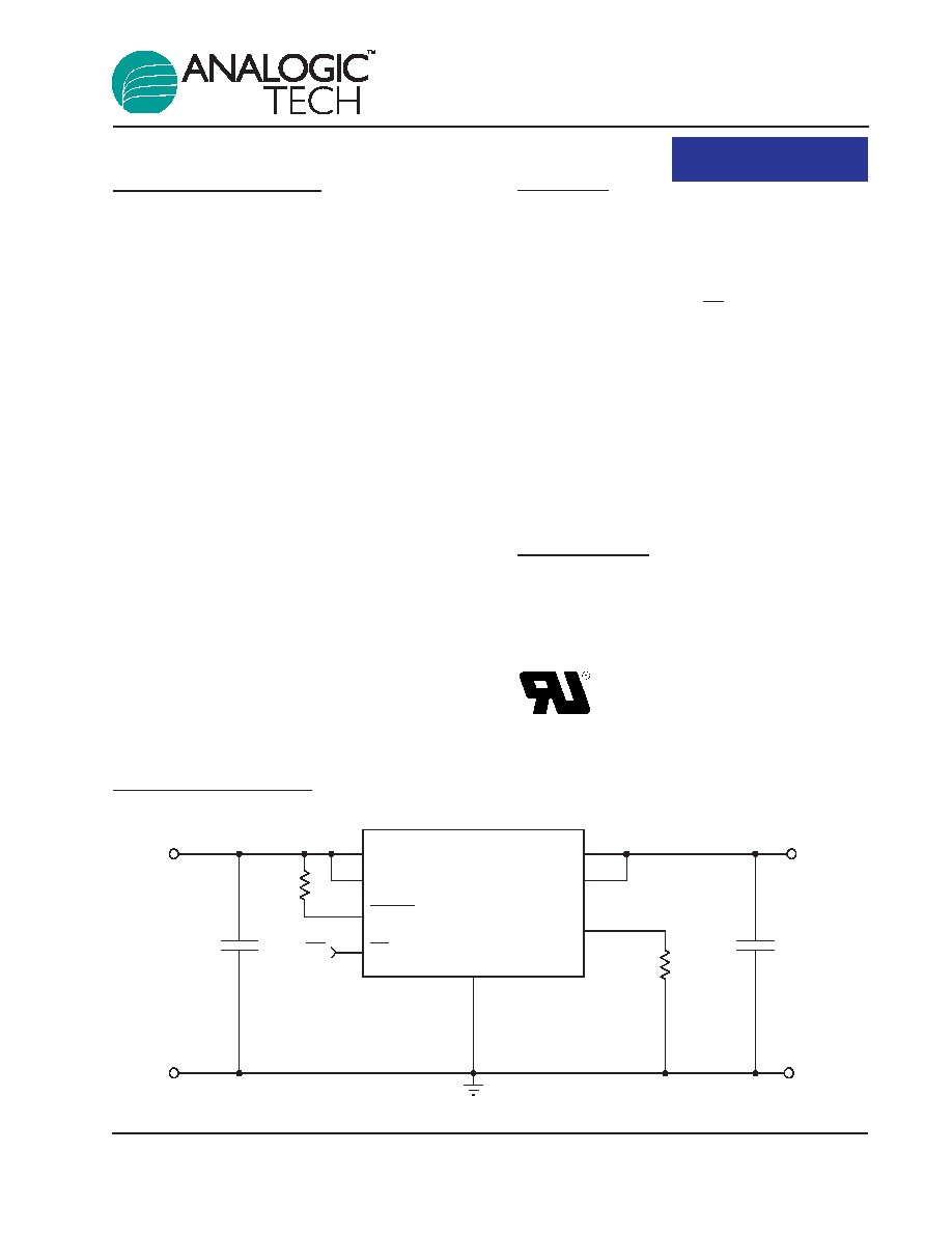
Typical Application
AAT4601A
ON
IN
OUT
SET
GND
ON
1ĶF
100k
R
SET
1ĶF
INPUT
OUTPUT
IN
OUT
FAULT
1
2
8
3
6
7
5
4

Pin Descriptions
Pin Configuration
SOP-8
MSOP-8
(Top View)
(Top View)
TSSOP-8
(Top View)
IN
IN
ON
GND
FAULT
OUT
OUT
SET
4
3
2
1
5
6
7
8
1
2
OUT
FAULT
OUT
SET
IN
IN
ON
GND
1
2
3
4
8
7
6
5
1
2
OUT
FAULT
OUT
SET
IN
IN
ON
GND
1
2
3
4
8
7
6
5
Pin #
Symbol
Function
1, 2
IN
These pins are the input to the P-channel MOSFET source. Connect a
1ĶF capacitor from IN to GND.
3
ON
Active low enable input. A logic low turns the switch on.
4
GND
Ground.
5
SET
Current limit set input. A resistor from SET to ground sets the current limit
for the switch.
6, 7
OUT
These pins are the P-channel MOSFET drain connection. Connect a 1ĶF
capacitor from OUT to GND.
8
FAULT
Fault indication output. This open-drain output goes low when in current
limit or when the die temperature exceeds +135ļC, with a 2ms delay after
the fault event occurs.
AAT4601A
1.8A Current Limited P-Channel Switch
2
4601A.2006.05.1.5
AAT4601A
1.8A Current Limited P-Channel Switch
4601A.2006.05.1.5
3
Absolute Maximum Ratings
1
T
A
= 25įC, unless otherwise noted.
Thermal Characteristics
3
Symbol
Description
Value
Units
SOP-8
100
JA
Maximum Thermal Resistance
TSSOP-8
150
įC/W
MSOP-8
150
SOP-8
1.25
W
P
D
Maximum Power Dissipation
TSSOP-8
833
mW
MSOP-8
833
Symbol
Description
Value
Units
V
IN
IN to GND
-0.3 to 6
V
V
ON,
V
FAULT
ON, FAULT to GND
-0.3 to V
IN
+ 0.3
V
V
SET,
V
OUT
SET, OUT to GND
-0.3 to V
IN
+ 0.3
V
I
MAX
Maximum Continuous Switch Current
3
A
T
J
Operating Junction Temperature Range
-40 to 150
įC
T
LEAD
Maximum Soldering Temperature (at Leads)
300
įC
V
ESD
ESD Rating--HBM
2
4000
V
1. Stresses above those listed in Absolute Maximum Ratings may cause permanent damage to the device. Functional operation at condi-
tions other than the operating conditions specified is not implied. Only one Absolute Maximum Rating should be applied at any one time.
2. Human body model is a 100pF capacitor discharged through a 1.5k
resistor into each pin.
3. Mounted on an FR4 printed circuit board.
AAT4601A
1.8A Current Limited P-Channel Switch
4
4601A.2006.05.1.5
Electrical Characteristics
V
IN
= 5V, T
A
= -40įC to +85įC, unless otherwise noted. Typical values are T
A
= 25įC.
Symbol
Description
Conditions
Min
Typ
Max
Units
V
IN
Operation Voltage
2.7
5.5
V
I
Q
Quiescent Current
V
IN
= 5V, ON = GND, I
OUT
= 0
12
30
ĶA
I
Q(OFF)
Off-Supply Current
ON = IN, V
IN
= 5.5V
0.004
1
ĶA
I
SD(OFF)
Off-Switch Current
ON = IN, V
IN
= 5.5V, V
OUT
= 0
0.07
15
ĶA
V
UVLO
Under-Voltage Lockout
Rising Edge, 1% Hysteresis
2.0
2.3
2.7
V
V
IN
= 5.0V
70
120
R
DS(ON)
On Resistance
V
IN
= 4.5V
75
130
V
IN
= 3.0V
80
150
m
V
IN
= 3.0V, T
A
= 25įC
80
110
I
LIM
Current Limit
R
SET
= 20.5k
750
1000
1250
mA
I
LIM(MIN)
Minimum Current Limit
260
mA
OTMP
Shutdown Temperature
V
IN
= 5V
125
ļC
V
ONL
ON Input Low Voltage
0.8
V
V
ONH
ON Input High Voltage
V
IN
= 2.7V to 3.6V
2.0
V
IN
= 4.5V to 5.5V
2.4
V
I
ONSINK
ON Input leakage
V
ON
= 5.5V
0.01
1
ĶA
V
FAULTL
FAULT Logic Output Low Voltage
I
SINK
= 1mA
0.08
0.4
V
I
FSINK
FAULT Logic Output High Leakage
V
FAULT
= 5.5V
0.05
1
ĶA
T
RESP
Current Limit Response Time
V
IN
= 5V
2
Ķs
T
BLANK
Fault Blanking Time After Turn-On
2
ms
T
OFF
Turn-Off Time
1
V
IN
= 5V
20
Ķs
T
ON
Turn-On Time
1
V
IN
= 5V
200
Ķs
1. Guaranteed by design.

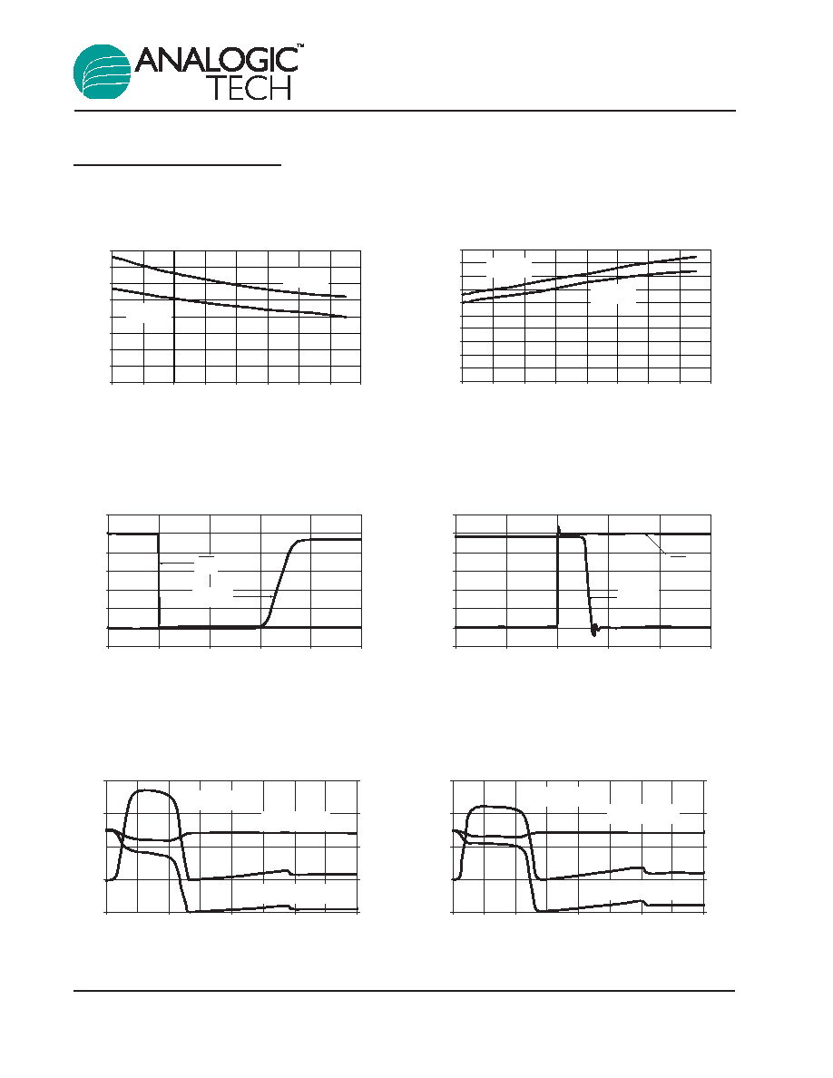
Typical Characteristics
Unless otherwise noted, V
IN
= 5V, T
A
= 25įC.
Off-Switch Current vs. Temperature
1
0.1
0.01
0.001
0.0001
10
-40
-20
0
20
40
60
80
100
120
140
Temperature (
įC)
Off-Switch Current (
A)
Off-Supply Current vs. Temperature
0.0001
0.001
0.01
0.1
1
10
-40
-20
0
20
40
60
80
100
120
140
Temperature
Off-Supply Current (
A)
(
įC)
R
SET
* I
LIM
Product vs. I
LIM
Typical I
LIM
(A)
Product (V)
18000
19000
20000
21000
22000
23000
24000
25000
0.0
0.5
1.0
1.5
2.0
2.5
Current Limit
(R
SET
= 20.5k
; V
IN
= 5.0V)
Output Voltage (V)
Output Current (A)
0.0
0.2
0.4
0.6
0.8
1.0
1.2
0
1
2
3
4
5
0
0
1
2
3
4
5
6
5
10
15
20
25
Quiescent Current
Input Voltage (V)
Input Curent (
A)
Quiescent Current vs. Temperature
0
5
10
15
20
25
-40
-20
0
20
40
60
80
100
120
Temperature (
įC)
Quiescent Current (
A)
AAT4601A
1.8A Current Limited P-Channel Switch
4601A.2006.05.1.5
5
AAT4601A
1.8A Current Limited P-Channel Switch
6
4601A.2006.05.1.5
Typical Characteristics
Unless otherwise noted, V
IN
= 5V, T
A
= 25įC.
Short-Circuit Through 0.6
0
2
4
6
8
-20
0
20
40
60
80
100
120
140
Time (
s)
Input and Output Voltage (V)
Output Current (A)
-3
0
3
6
9
Output Current
Input Voltage
Output Voltage
Short-Circuit Through 0.3
0
2
4
6
8
0
2
4
6
8
Time (
s)
Input and Output Voltage (V)
Output Current (A)
-4
0
4
8
12
Output Current
Input Current
Output Current
Switch Turn-Off Time
(I
OUT
= I
LIMIT
)
-1
0
1
2
3
4
5
6
-4
-2
0
2
4
6
Time (
s)
Voltage (V)
Output
ON
Switch Turn-On Time
(I
OUT
= I
LIMIT
)
-1
0
1
2
3
4
5
6
-20
-10
0
40
60
80
Time (
s)
Voltage (V)
Output
ON
Turn-Off Time vs. Temperature
0
0.2
0.4
0.6
0.8
1.0
1.8
1.6
1.4
1.2
2.0
-40
-20
0
20
40
60
80
100
120
Temperature (
įC)
Turn-Off Time (
s)
V
IN
= 5V
V
IN
= 3V
Turn-On Time vs. Temperature
0
10
20
30
40
50
60
70
80
-40
-20
0
20
40
60
80
100
120
Temperature (
įC)
Turn-On Time (
s)
V
IN
= 3V
V
IN
= 5V

Typical Characteristics
Unless otherwise noted, V
IN
= 5V, T
A
= 25įC.
R
DS(ON)
vs. Temperature
40
50
60
70
80
90
100
-40
-20
0
20
40
60
80
Temperature (
įC)
R
DS(ON)
(m
)
V
IN
= 4.5V
V
IN
= 3V
Fault Delay vs. Temperature
0
0.5
1.0
1.5
2.0
2.5
-40
-20
0
20
40
60
80
100
Temperature (
įC)
Fault Delay (ms)
AAT4601A
1.8A Current Limited P-Channel Switch
4601A.2006.05.1.5
7

AAT4601A
1.8A Current Limited P-Channel Switch
8
4601A.2006.05.1.5
Functional Block Diagram
IN
ON
SET
FAULT
OUT
Under-
Voltage
Lockout
Over-Temperature
Protection
1.2V
Reference
Current
Limit
Functional Description
The AAT4601A is an integrated MOSFET load
switch with an adjustable current limit, over-tem-
perature protection, level-shifted input, and a fault
flag. The current limit control is combined with an
over-temperature thermal limit circuit to provide a
comprehensive system to protect the load switch
under short-circuit or other adverse operating con-
ditions. The AAT4601A is ideally suited for control
and protection of peripheral ports such as USB,
RS232, and parallel ports.
The current limit and over-temperature circuits will
act independently. The device current limit is acti-
vated when the output load current exceeds an
internal threshold level. The internal current limit
threshold is determined by an external resistor
connected between the SET pin and ground. The
minimum current limit threshold is specified by
I
LIM(MIN)
. If the load switch ambient temperature
becomes excessive or if a short-circuit condition
persists, the die temperature will rise causing the
over-temperature protection circuit to activate.
If a current limit level less than I
LIM(MIN)
is required,
the AAT4601A can be used to operate in foldback
current limit mode. To achieve this, an R
SET
value
can be chosen to program a current limit lower
than I
LIM(MIN)
; in this case, when the load current
reaches I
LIM(MIN)
, the current will immediately drop,
limiting at the programmed value.
If the current limit or over-temperature protection
circuits are active for more than 2ms, the system
will be informed via the FAULT flag. The 2ms delay
allows the AAT4601A to be turned on into capaci-
tive loads without activating the FAULT flag. The
open drain FAULT output can be connected direct-
ly to system controllers driven by voltage levels
less than the IN pin voltage without additional level
shifting circuitry.
The load switch is turned off by applying a logic high
level to the ON pin. The AAT4601A typically con-
sumes 12ĶA when operating; when off, the device
draws less than 1ĶA. In the off state, current is pre-
vented from flowing between the input and output.
The ON function has logic level thresholds that
allow the AAT4601A to be TTL compatible and may
also be controlled by 2.5V to 5.0V CMOS circuits.
The voltage level on either ON or FAULT should not
exceed the input supply level present on the IN pin.
Applications Information
Setting Current Limit
A simple three-step procedure can be used to
adjust the AAT4601A's current limit. First, the max-
imum current required by the load should be deter-
mined. Second, select a resistor that guarantees
adequate current is available to the load under nor-
mal conditions. Finally, the maximum current that
can pass through the switch can be calculated and
compared to the maximum current available.
Step 1: The maximum current required by a load
is usually defined in port specifications design
application references. For example, USB ports
may be specified to support loads of up to 500mA.
Step 2: The most convenient method for deter-
mining a current limit resistor value is to look it up
in Table 1, "Current Limit R
SET
Values." Find the
lowest current value that is greater than the maxi-
mum load current in the given application as listed
in the column, "Device Will Not Current Limit
Below." The resistor value needed is listed in the
corresponding row in the column, "R
SET
." For
example, a USB port requires 500mA. The lowest
level where the device will current limit above
500mA is 507mA. The corresponding resistor
value for R
SET
would be 33k
.
Step 3: Now the required resistor value has been
determined. The maximum current that can be
drawn, even with a short circuit applied to the out-
put, can be determined by reading the column,
"Device Always Current Limits Below." If the power
supply connected to the AAT4601A's input can pro-
vide this current level, the power supply voltage will
not collapse when a short circuit is applied to the
load switch output. For example, a notebook com-
puter has a USB port which is powered by an
AAT4601A with a 33k
resistor connected between
the SET pin and GND. If the power supply con-
nected to the AAT4601A's IN pin can provide more
than 845mA, this supply will remain in regulation
even if a short circuit is applied to the USB port.
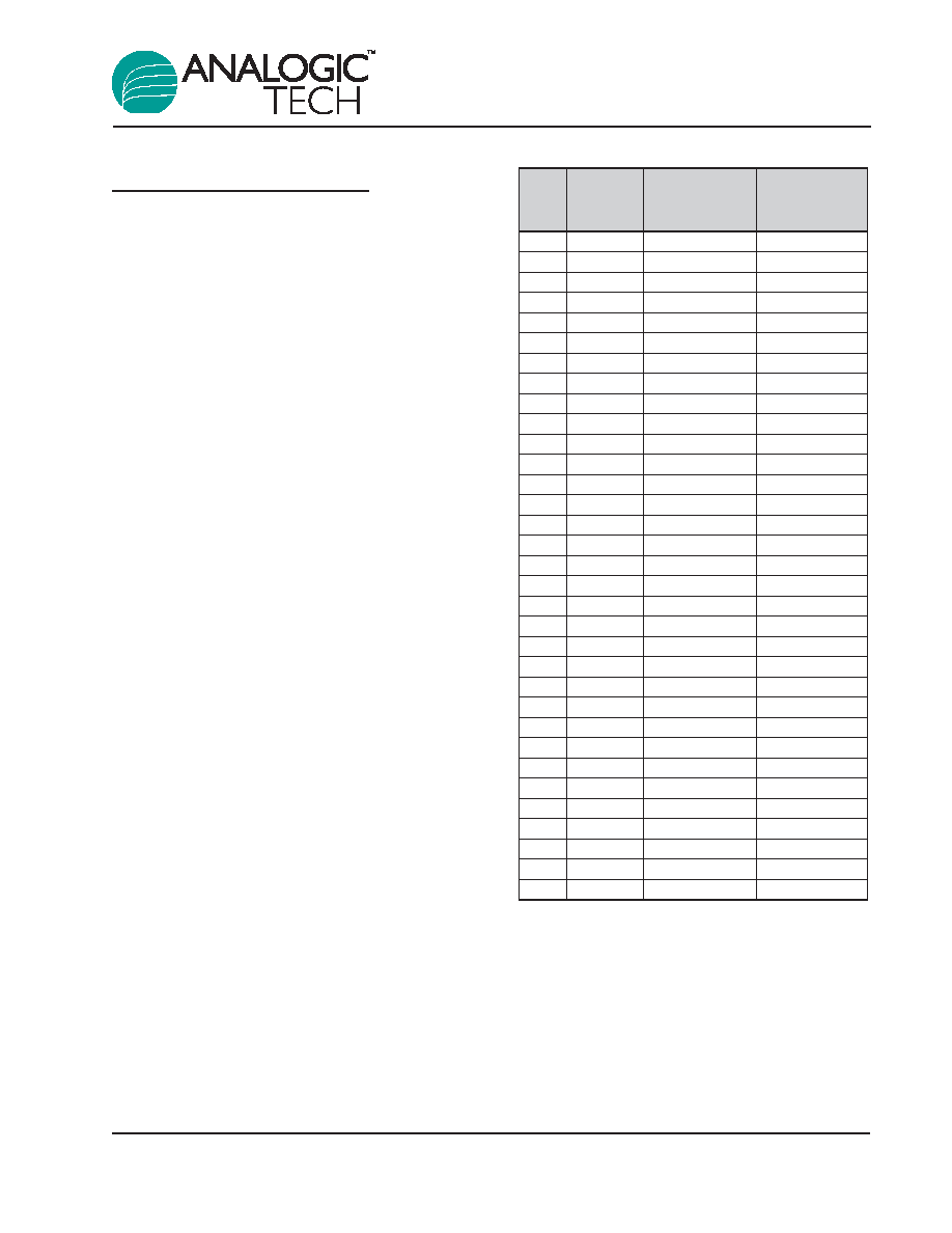
Figure 1: Current Limit R
SET
Values.
AAT4601A
1.8A Current Limited P-Channel Switch
4601A.2006.05.1.5
9
Current
Device Will Not Device Always
R
SET
Limit
Current Limit Current Limits
(k
) Typ (mA)
Below (mA)
Below (mA)
7.5
2476
1857
3095
8.2
2277
1708
2847
9.1
2065
1549
2581
10
1895
1421
2369
11
1748
1311
2185
12
1633
1224
2041
13
1528
1146
1910
15
1353
1015
1691
16
1280
960
1600
18
1158
869
1448
20
1055
791
1318
22
972
729
1215
24
897
673
1122
27
811
608
1014
30
736
552
919
33
676
507
845
36
625
469
781
39
582
436
727
43
533
400
666
47
491
368
613
51
455
341
568
56
418
314
523
62
380
285
476
68
350
262
437
75
320
240
400
82
295
221
369
91
267
200
334
100
245
183
306
110
223
167
279
120
206
155
258
130
192
144
239
150
167
125
209
160
157
118
197

AAT4601A
1.8A Current Limited P-Channel Switch
10
4601A.2006.05.1.5
Operation in Current Limit
If an excessive load is applied to the output of an
AAT4601A, the load current will be limited by the
device's current limit circuitry as shown in Figure 1,
"Overload Operation." If a short circuit were to occur
on the load, it would demand more current than
allowed by the internal current limiting circuit and the
voltage at the AAT4601A's output would drop. This
causes the AAT4601A to dissipate more power than
in normal operation, causing the die temperature to
increase. When die temperature exceeds the internal
over-temperature threshold, the AAT4601A will shut
down. After shutting down, the AAT4601A cools to a
level below the over-temperature threshold, at which
point it will start up again. The AAT4601A will contin-
ue to cycle off and on until one of the following events
occurs: the load current is reduced to a level below
the AAT4601A's current limit setting; the input power
is removed; or the output is turned off by a logic high
level applied to the ON pin.
Thermal Considerations
Since the AAT4601A has internal current limit and
over-temperature protection, junction temperature is
rarely a concern. If an application requires a large
load current in a high-temperature operating envi-
ronment, there is the possibility that the over-tem-
perature protection circuit, rather than the current
limit circuit, will regulate the current available to the
load. In these applications, the maximum current
available without risk of activation of the over-tem-
perature circuit can be calculated. The maximum
internal temperature while current limit is not active
can be calculated using Equation 1:
Eq. 1:
In Equation 1, I
MAX
is the maximum current required
by the load. R
DS(ON)(MAX)
is the maximum rated
R
DS(ON)
of the AAT4601A at high temperature. R
JA
is
the thermal resistance between the AAT4601A's die
and the board onto which it is mounted. T
A(MAX)
is the
maximum ambient temperature for the printed circuit
board assembly under the AAT4601A when the load
switch is not dissipating power. Equation 1 can be
transformed to provide I
MAX
; refer to Equation 2:
Eq. 2:
T
SD(MIN)
is the minimum temperature required to
activate the AAT4601A's over-temperature protec-
tion. With a typical specification of 125įC, 115įC is
a safe minimum value to use.
=
I
MAX
T
SD(MIN)
- T
A(MAX)
R
DS(ON)(MAX)
◊ R
JA
T
J(MAX)
= I
MAX
2
◊ R
DS(ON)(MAX)
◊ R
JA
+ T
A(MAX)
Figure 1: Overload Operation.
0
1
2
3
4
5
6
-0.5
0
0.5
1
1.5
2
Time (s)
Voltage (V)
Output Voltage
Input Voltage
1
is Applied to Output at t = 0
R
SET
is 33k
For example, a portable device is specified to oper-
ate in a 50įC environment. The printed circuit
board assembly will operate at temperatures as
high as 85įC. This portable device has a sealed
case and the area of the printed circuit board
assembly is relatively small, causing R
JA
to be
approximately 120įC/W. Using Equation 2:
Eq. 3:
If this system requires less than 1.4A, the thermal
limit will not activate during normal operation.
Input Capacitor
The input capacitor serves two purposes. First, it
protects the source power supply from transient
current effects generated by the application load
circuit. If a short circuit is suddenly applied to the
output of an AAT4601A, there is a microsecond-
long period during which a large current can flow
before the current limit circuitry activates; refer to
the characteristic curve, "Short-Circuit Through
0.3
." A properly sized input capacitor can dramat-
ically reduce the load switch input transient
response effects seen by the power supply and
other circuitry upstream from the AAT4601A.
The second purpose of the input capacitor is to
prevent transient events generated by the load cir-
cuit from affecting operation of the AAT4601A. For
example, if an AAT4601A is used in a circuit that
operates from a 3V power supply with poor step
load response, it is possible that turning on the load
switch could cause the input power supply to droop
below the AAT4601A's under-voltage lockout
threshold. This drop in voltage would cause the
AAT4601A to turn off until the input power supply's
voltage recovers. Since this cycle would be self-
perpetuating, the entire circuit could be seen to be
unstable. In the very rare case where capacitor
cost is prohibitive, the output load circuit should be
slew rate limited when turned on.
Output Capacitor
In order to insure stability while the device current
limit is active, a small capacitance of approximately
1ĶF should be used. When the AAT4601A is acti-
vated using the ON function, there are no momen-
tary current transients, as in the case when a short
circuit is suddenly applied to a device that is already
on; refer to the characteristic curve, "Switch Turn-On
Time." No matter how big the output capacitor, out-
put current is limited to the value allowed by the
threshold determined by R
SET
and the internal cur-
rent limiting circuitry. This permits very large output
capacitors to be used.
For example, USB ports are specified to have at least
120ĶF of downstream capacitance from their control-
ling power switch. An output capacitance as large as
1000ĶF would not disturb the input power supply to
the AAT4601A used to control the USB port.
ON Input
When the AAT4601A is in the off state, the output
is an open circuit and the device quiecent current
consumption is reduced to less than 1ĶA. The ON
threshold voltage is set to allow the AAT4601A to
be controlled by 5V TTL levels as well as CMOS
power from 2.5V to 5V. The ON function control
voltage level should not exceed the input supply
level applied to the IN pin.
FAULT Output
A FAULT flag is provided to alert a system if the load
switch is not receiving a sufficient voltage level to
properly operate. If either the current limit or over-
temperature circuits in any combination are contin-
uously active for more than approximately 2ms, the
FAULT pin is pulled to ground internally through a
100
resistance. The 2ms delay on the FAULT
function is intended to prevent capacitive loads con-
nected to the load switch output from activating
FAULT when the device is turned on. The place-
ment of a pull-up resistor between the FAULT pin
and the IN pin is recommended. Reasonable val-
ues for the pull-up resistor should range from 10k
to 100k
. Since FAULT is an open drain terminal,
=
I
MAX
= 1.4A
115 - 85
130 ∑ 120
AAT4601A
1.8A Current Limited P-Channel Switch
4601A.2006.05.1.5
11
AAT4601A
1.8A Current Limited P-Channel Switch
12
4601A.2006.05.1.5
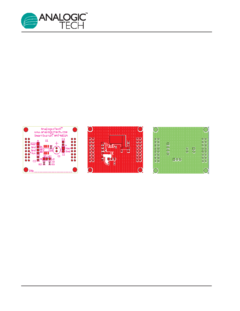
Figure 1: AAT4601A Evaluation
Figure 2: AAT4601A Evaluation
Figure 3: AAT4601A Evaluation
Board Top Side Silk Screen
Board Component Side Layout.
Board Solder Side Layout.
Assembly Drawing.
it may be pulled up to any voltage that is not greater
than the level present on the IN pin. This is done to
allow the AAT4601A to signal ancillary circuitry that
is powered by a voltage level less than the level on
the IN pin.
Reverse Voltage
The AAT4601A is designed to control current flow-
ing from IN to OUT. If a voltage is applied to OUT
that is greater than that on IN, a large resulting
reverse current may flow, potentially damaging the
AAT4601A.
Printed Circuit Board Layout
Recommendations
For proper thermal management, and to take
advantage of the low R
DS(ON)
of the AAT4601A, a
few circuit board layout rules should be followed:
V
IN
and V
OUT
should be routed using wider than
normal traces, and GND should be connected to a
ground plane. For best performance, C
IN
and C
OUT
should be placed close to the package pins.
Evaluation Board Layout
The AAT4601A evaluation layout follows the print-
ed circuit board layout recommendations and can
be used for good applications layout.
Note: Board layout shown is not to scale.
Ordering Information
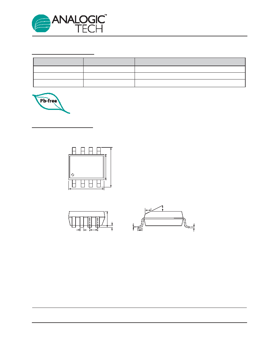
Package Information
SOP-8
All dimensions in millimeters.
0.175
Ī
0.075
6.00
Ī
0.20
3.90
Ī
0.10
1.55
Ī
0.20
1.27 BSC
0.42
Ī 0.09 ◊ 8
4.90
Ī 0.10
4
į
Ī
4
į
45
į
0.375
Ī 0.125
0.235
Ī 0.045
0.825
Ī 0.445
All AnalogicTech products are offered in Pb-free packaging. The term "Pb-free" means
semiconductor products that are in compliance with current RoHS standards, including
the requirement that lead not exceed 0.1% by weight in homogeneous materials. For more
information, please visit our website at http://www.analogictech.com/pbfree.
Package
Marking
1
Part Number (Tape and Reel)
2
SOP-8
4601A
AAT4601AIAS-T1
TSSOP-8
4601A
AAT4601AIHS-T1
MSOP-8
MQXYY
AAT4601AIKS-T1
AAT4601A
1.8A Current Limited P-Channel Switch
4601A.2006.05.1.5
13
1. XYY = assembly and date code.
2. Sample stock is generally held on part numbers listed in BOLD.

TSSOP-8
All dimensions in millimeters.
DETAIL A
4.40
Ī
0.10
6.40
Ī
0.20
0.65 BSC
3.00
Ī 0.10
0.245
Ī 0.055 ◊ 8
0.10
Ī 0.05
0.60
Ī 0.15
0.145
Ī 0.055
1.05 MAX
1.20 MAX
4
į Ī 4į
12
į
12
į REF ◊ 4
1.00
REF
AAT4601A
1.8A Current Limited P-Channel Switch
14
4601A.2006.05.1.5

MSOP-8
All dimensions in millimeters.
PIN 1
1.95 BSC
0.254 BSC
0.155
Ī 0.075
0.60
Ī 0.20
3.00
Ī
0.10
0.95
Ī
0.15
0.95 REF
0.85
Ī
0.10
3.00
Ī 0.10
10
į Ī 5į
4
į Ī 4į
0.65 BSC
0.30
Ī 0.08
0.075
Ī 0.075
4.90
Ī
0.10
GAUGE PLANE
AAT4601A
1.8A Current Limited P-Channel Switch
4601A.2006.05.1.5
15

AAT4601A
1.8A Current Limited P-Channel Switch
16
4601A.2006.05.1.5
Advanced Analogic Technologies, Inc.
830 E. Arques Avenue, Sunnyvale, CA 94085
Phone (408) 737-4600
Fax (408) 737-4611
© Advanced Analogic Technologies, Inc.
AnalogicTech cannot assume responsibility for use of any circuitry other than circuitry entirely embodied in an AnalogicTech product. No circuit patent licenses, copyrights, mask work rights,
or other intellectual property rights are implied. AnalogicTech reserves the right to make changes to their products or specifications or to discontinue any product or service without notice.
Customers are advised to obtain the latest version of relevant information to verify, before placing orders, that information being relied on is current and complete. All products are sold sub-
ject to the terms and conditions of sale supplied at the time of order acknowledgement, including those pertaining to warranty, patent infringement, and limitation of liability. AnalogicTech
warrants performance of its semiconductor products to the specifications applicable at the time of sale in accordance with AnalogicTech's standard warranty. Testing and other quality con-
trol techniques are utilized to the extent AnalogicTech deems necessary to support this warranty. Specific testing of all parameters of each device is not necessarily performed.
AnalogicTech and the AnalogicTech logo are trademarks of Advanced Analogic Technologies Incorporated. All other brand and product names appearing in this document are regis-
tered trademarks or trademarks of their respective holders.