SmartSwitch
TM
General Description
The AAT4601
SmartSwitchTM
is
part
of
AnalogicTech's
Application
Specific
Power
MOSFETTM (ASPMTM) product family. It is a 1.5A
Current Limited P-channel MOSFET power switch
designed for high-side load-switching applications.
This switch operates with inputs ranging from 2.7V
to 5.5V, making it ideal for both 3V and 5V sys-
tems. An integrated current-limiting circuit protects
the input supply against large changes in load cur-
rent which could cause the supply to fall out of reg-
ulation. The AAT4601 has protection from thermal
overload which limits power dissipation and junc-
tion temperatures. The maximum current limit
level is 1.5A; the actual threshold is programmed
with a resistor from the SET pin to ground. The qui-
escent supply current is typically 12µA. In shut-
down mode, the supply current decreases to less
than 1µA.
The AAT4601 is available in 8-pin SOP or TSSOP
specified over -40 to 85∞C.
Features
∑
2.7V to 5.5V Input voltage range
∑
Programmable over current threshold
∑
Low quiescent current
∑
12µA typical
∑
Less than 1µA with Switch off
∑
Only 2.5V needed for ON Control
∑
Thermal Shutdown
∑
Fault Flag
∑
2ms Fault Blanking
∑
Undervoltage Lockout
∑
Temperature range -40 to 85∞C
∑
2kV ESD rating
∑
UL Approved--File No. E217765
∑
8-pin SOP or TSSOP package
Applications
∑
USB ports
∑
Notebook computers
∑
Peripheral ports
∑
Hot swap supplies
UL Recognized Component
AAT4601
1.5A Current Limited P-Channel Switch
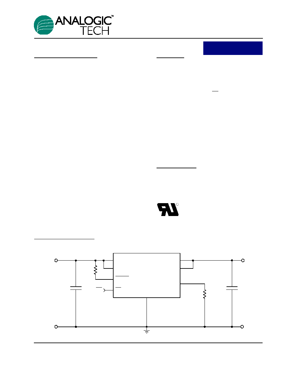
Typical Application
AAT4601
ON
IN
OUT
SET
GND
ON
1
µ
F
100k
R
SET
1uF
INPUT
OUTPUT
IN
OUT
FAULT
1
2
8
3
6
7
5
4
Preliminary
Information
4601.2001.11.0.92
1

Pin Descriptions
Pin Configuration
SOP-8/TSSOP-8
(Top View)
1
2
IN
ON
GND
FAULT
OUT
OUT
SET
IN
1
2
3
4
8
7
6
5
Pin #
Symbol
Function
1,2
IN
These pins are the input to the P-channel MOSFET source. Connect a
1µF capacitor from IN to GND.
3
ON
Active-Low Enable Input. A logic low turns the switch on.
4
GND
Ground
5
SET
Current-Limit Set Input. A resistor from SET to ground sets the current
limit for the switch.
6,7
OUT
These pins are the P-channel MOSFET drain connection. Connect a 1µF
capacitor from OUT to GND.
8
FAULT
Fault-Indication Output. This open-drain output goes low when in current
limit or when the die temperature exceeds +135 ∫C, with a 2ms delay
after the fault event occurs.
AAT4601
1.5A Current Limited P-Channel Switch
2
4601.2001.11.0.92
AAT4601
1.5A Current Limited P-Channel Switch
4601.2001.11.0.92
3
Absolute Maximum Ratings
(T
A
=25∞C unless otherwise noted)
Note: Stresses above those listed in Absolute Maximum Ratings may cause permanent damage to the device. Functional operation at con-
ditions other than the operating conditions specified is not implied. Only one Absolute Maximum rating should be applied at any one time.
Note 1: Human body model is a 100pF capacitor discharged through a 1.5k
resistor into each pin.
Thermal Characteristics
Note 2: Mounted on an AATI demo board.
Electrical Characteristics
(V
IN
= 5V, T
A
= -40 to 85∞C unless otherwise noted. Typical values
are at T
A
=25∞C)
Note 3: Guaranteed by design.
Symbol
Description
Conditions
Min
Typ
Max
Units
V
IN
Operation Voltage
2.7
5.5
V
I
Q
Quiescent Current
V
IN
= 5V, ON = GND, I
OUT
= 0
12
30
µA
I
Q(OFF)
Off Supply Current
ON=IN, V
IN
= 5.5V
.004
1
µA
I
SD(OFF)
Off Switch Current
ON = IN, V
IN
= 5.5V, V
OUT
= 0
.07
15
µA
V
UVLO
Undervoltage Lockout
Rising edge, 1% hysteresis,
2.0
2.3
2.7
V
V
IN
=5.0V
70
m
R
DS(ON)
On-Resistance
V
IN
=4.5V
75
130
m
V
IN
=3.0V
80
150
m
I
LIM
Current Limit
R
SET
= 2k
510
715
920
mA
I
LIM(MIN)
Minimum Current Limit
250
mA
TSD
Shutdown Temperature
V
IN
= 5V
125
∫C
V
ONL
ON Input Low Voltage
0.8
V
V
ONH
ON Input High Voltage
V
IN
=2.7V to 3.6V
2.0
V
V
IN
=4.5V to 5.5V
2.4
V
I
ONSINK
ON Input leakage
V
ON
= 5.5V
0.01
1
µA
V
FAULTL
FAULT Logic Output Low Voltage
I
SINK
=1mA
0.08
0.4
V
I
FSINK
FAULT Logic Output High Leakage
V
FAULT
= 5.5V
0.05
1
µA
T
RESP
Current Limit Response Time
V
IN
=5V
2
µs
T
BLANK
Fault Blanking Time after Turn-On
2
ms
T
OFF
Turn-Off Time
3
V
IN
=5V
20
µs
T
ON
Turn-On Time
3
V
IN
=5V
200
µs
OTMP
Over Temperature Shut Down
125
∫C
Symbol
Description
Value
Units
JA
Typical Thermal Resistance
2
100
∞C/W
P
D
Maximum Power Dissipation
2
1.25
W
Symbol
Description
Value
Units
V
IN
IN to GND
-0.3 to 6
V
V
ON,
V
FAULT
ON, FAULT to GND
-0.3 to V
IN
+0.3
V
V
SET,
V
OUT
SET, OUT to GND
-0.3 to V
IN
+0.3
V
I
MAX
Maximum Continuous Switch Current
3
A
T
J
Operating Junction Temperature Range
-40 to 150
∞C
T
LEAD
Maximum Soldering Temperature (at Leads)
300
∞C
V
ESD
ESD Rating--HBM
1
4000
V
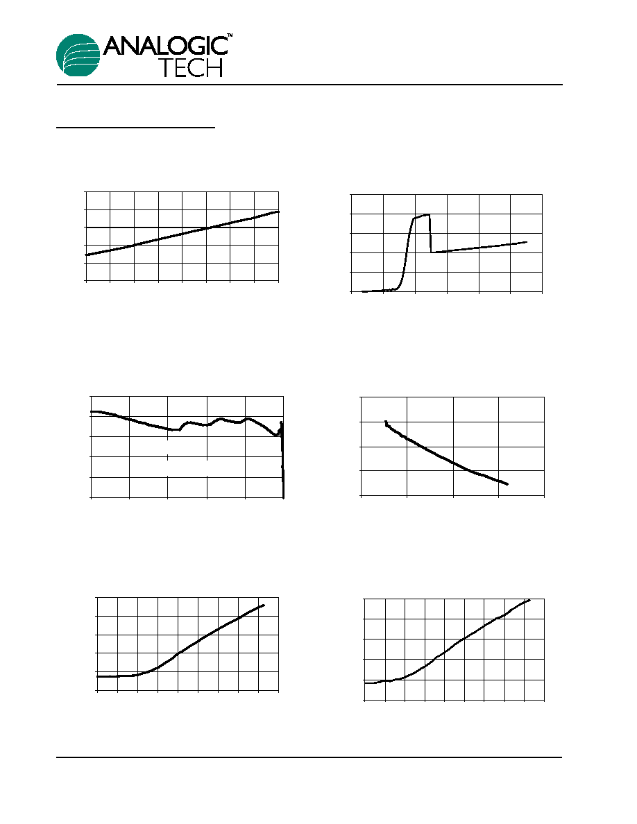
Typical Characteristics
(Unless otherwise noted, V
IN
= 5V, T
A
= 25∞C)
Off-Switch Current vs. Temperature
1
0.1
0.01
0.001
0.0001
10
-40
-20
0
20
40
60
80
100
120
140
Temperature (
∞
C)
Off-Switch Current (
µ
A)
Off-Supply Current vs. Temperature
0.0001
0.001
0.01
0.1
1
10
-40
-20
0
20
40
60
80
100
120
140
Temperature
Off-Supply Current (
µ
A)
(
∞
C)
R
SET
I
LIM
Product vs I
LIM
500
1000
1500
2000
2500
0
0.5
1
1.5
2
Typical I
LIM
(A)
Product (V)
Current Limit
0
0.2
0.4
0.6
0.8
1
0
1
2
3
4
5
Output (V)
Output (A)
R
SET
= 2 k
9
Input Voltage = 5 V
0
0
1
2
3
4
5
6
5
10
15
20
25
Quiescent Current
Input (V)
Input (
µ
A)
Quiescent Current vs. Temperature
0
5
10
15
20
25
-40
-20
0
20
40
60
80
100
120
Temperature
Quiescent Current (
µ
A)
(
∞
C)
AAT4601
1.5A Current Limited P-Channel Switch
4
4601.2001.11.0.92

Typical Characteristics
(Unless otherwise noted, V
IN
= 5V, T
A
= 25∞C)
Short Circuit through 0.6
0
2
4
6
8
-20
0
20
40
60
80
100
120
140
Time (
µ
s)
Input
and
Output
-3
0
3
6
9
Output (A)
Output Current
Input Voltage
Output Voltage
(V)
Short Circuit through 0.3
0
2
4
6
8
0
2
4
6
8
Time (
µ
s)
Input
and
Output
-4
0
4
8
12
Outpu
t (A)
Output Current
Input Voltage
Output Voltage
(V)
Switch Turn-Off Time
-1
0
1
2
3
4
5
6
-4
-2
0
2
4
6
Time (
Voltage
(V)
Output
ON
I
OUT
= I
LIMIT
Switch Turn-On Time
-1
0
1
2
3
4
5
6
-20
-10
0
40
60
80
Time (
Voltage
(V)
Output
ON
I
OUT
=I
LIMIT
Turn-Off vs. Temperature
0
0.2
0.4
0.6
0.8
1
1.8
1.6
1.4
1.2
2
-40
-20
0
20
40
60
80
100
120
Temperature (
∞
C)
Turn-OFF
Time
(
µ
s)
V
IN
=5V
V
IN
=3V
Turn-On vs. Temperature
0
10
20
30
40
50
60
70
80
-40
-20
0
20
40
60
80
100
120
Temperature (
∞
C)
Turn-ON
Time
(
µ
s)
V
IN
= 3V
V
IN
= 5V
AAT4601
1.5A Current Limited P-Channel Switch
4601.2001.11.0.92
5
Typical Characteristics
(Unless otherwise noted, V
IN
= 5V, T
A
= 25∞C)
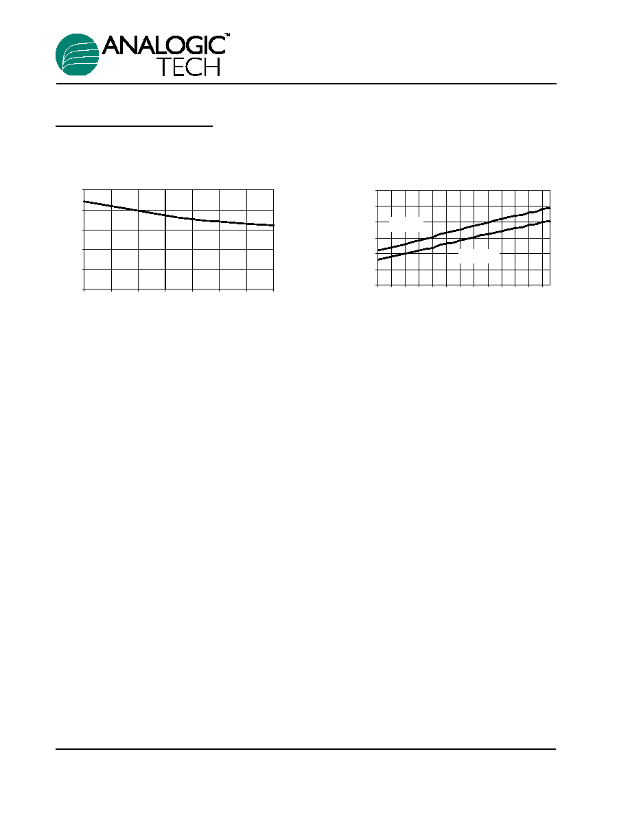
R
DS(ON)
vs. Temperature
40
50
60
70
80
90
100
-4 0
-20
0
20
40
60
80
Temperature (
∞
C)
R
DS(ON)
(m
)
V
IN
=4.5V
V
IN
=3V
Fault Delay vs. Temperature
0
0.5
1.0
1.5
2.0
2.5
-40
-20
0
20
40
60
80
100
Temperature (
∞
C)
Fault
Delay
(ms)
AAT4601
1.5A Current Limited P-Channel Switch
6
4601.2001.11.0.92
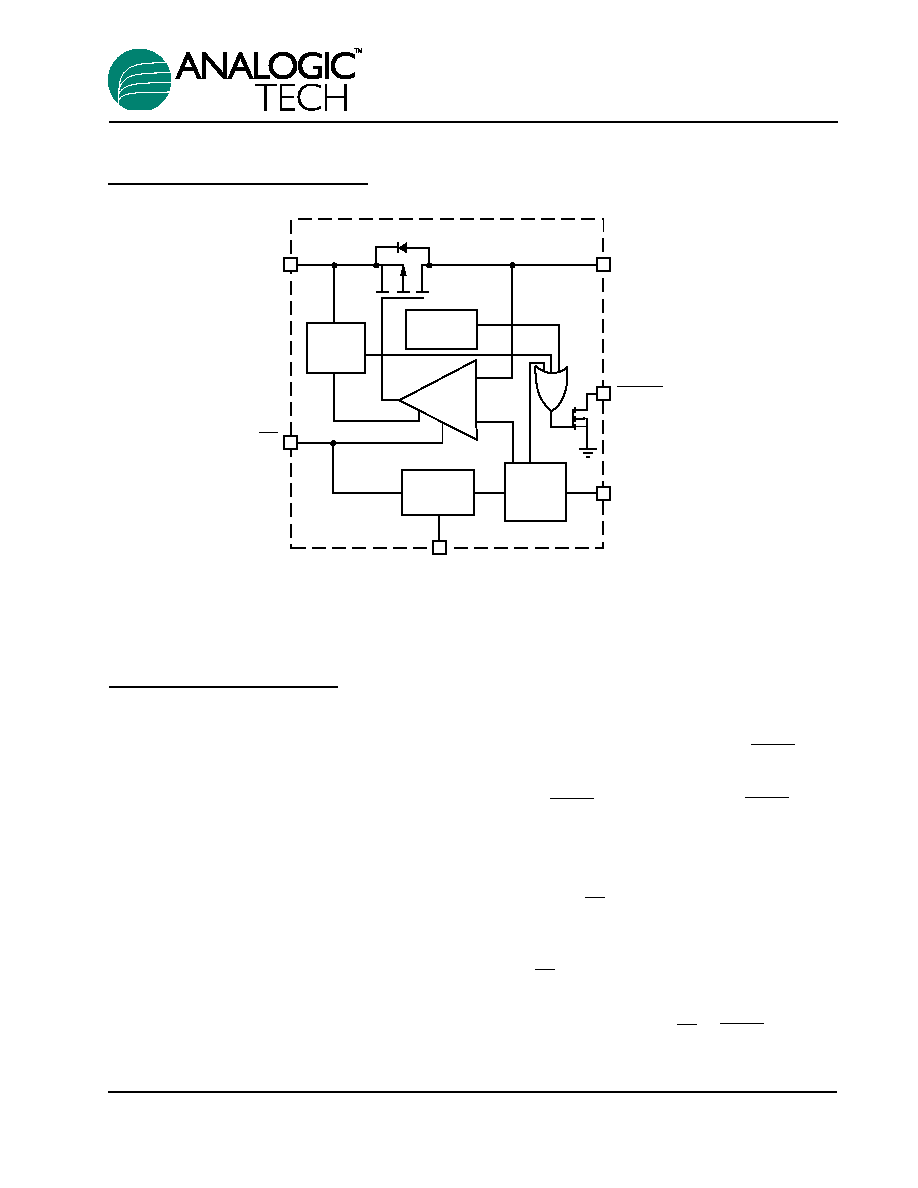
Functional Block Diagram
IN
ON
SET
FAULT
OUT
Under-
voltage
Lockout
Over-temp
Protection
1.2V
Reference
Current
Limit
AAT4601
1.5A Current Limited P-Channel Switch
4601.2001.11.0.92
7
Functional Description
The AAT4601 is an integrated MOSFET load
switch with an adjustable current limit, over tem-
perature protection, level shifted input and a fault
flag. The current limit control is combined with an
over temperature thermal limit circuit to provide a
comprehensive system to protect the load switch
under short circuit or other adverse operating con-
ditions. The AAT4601 is ideally suited for control
and protection of peripheral ports such as USB,
RS232 and parallel ports.
The current limit and over temperature circuits will
act independently. The device current limit is acti-
vated when the output load current exceeds an
internal threshold level. The internal current limit
threshold is determined by an external resistor
connected between the SET pin and ground. The
minimum current limit threshold is specified by
I
LIM(MIN)
. If the load switch ambient temperature
becomes excessive or if a short circuit condition
persists, the die temperature will rise causing the
over temperature protection circuit to activate.
If the current limit or over temperature protection
circuits are active for more then two milliseconds,
the system will be informed via the FAULT Flag.
The two millisecond delay allows the AAT4601 to
be turned on into capacitive loads without activat-
ing the FAULT Flag. The open drain FAULT output
can be connected directly to system controllers
driven by voltage levels less than the IN pin voltage
without additional level shifting circuitry.
The load switch is turned off by applying a logic high
level to the ON pin. The AAT4601 typically con-
sumes 12µA when operating, when off, the device
draws less then 1µA. In the off state, current is pre-
vented from flowing between the input and output.
The ON function has logic level thresholds that
allow the AAT4601 to be TTL compatible and may
also be controlled by 2.5V to 5.0V CMOS circuits.
The voltage level on either ON or FAULT should not
exceed the input supply level present on the IN pin.

Applications Information
Setting Current Limit
A simple three-step procedure can be used to
adjust the AAT4601's current limit. First, the maxi-
mum current required by the load should be deter-
mined. Second, select a resistor that guarantees
adequate current is available to the load under nor-
mal conditions. Finally, the maximum current that
can pass through the switch can be calculated and
compared to the maximum current available.
Step 1: The maximum current required by a load
is usually defined in port specifications design
application references. For example, USB ports
are specified to support loads of up to 500 mA.
Step 2: The most convenient method for deter-
mining a current limit resistor value is to look it up
in the provided table named "Current Limit R
SET
Values". Find the lowest current value that is
greater than the maximum load current in the given
application. Refer to the column named "Device
will not current limit below". The resistor value
needed is in the corresponding row named "R
SET
".
For example, a USB port requires 500 mA. The
lowest level where the device will current limit
above 500 mA is 516 mA. The corresponding
resistor value for R
SET
would be 2k
.
Step 3: Now the required resistor value has been
determined. The maximum current that can be
drawn, even with a short circuit applied to the out-
put, can be determined by reading the column
labeled "Device always current limits below". If the
power supply connected to the AAT4601's input can
provide this current level, the power supply voltage
will not collapse when a short circuit is applied to the
load switch output. For example, a notebook com-
puter has a USB port which is powered by an
AAT4601 with a 2k
resistor connected between
the SET pin and GND. If the power supply con-
nected to the AAT4601's IN pin can provide more
than 917 mA, this supply will remain in regulation
even if a short circuit is applied to the USB port.
Current Limit R
SET
Values
AAT4601
1.5A Current Limited P-Channel Switch
8
4601.2001.11.0.92
R
SET
Current
Device will
Device always
(
)
Limit typ not current
current limits
(mA)
limit below:
below:
(mA)
(mA)
470
1585
1141
2029
510
1529
1101
1957
560
1466
1055
1876
620
1397
1006
1788
680
1334
960
1707
750
1266
911
1620
820
1206
869
1544
910
1144
823
1464
1000
1089
784
1394
1100
1034
745
1324
1200
986
710
1262
1300
941
677
1204
1500
865
623
1107
1600
829
597
1061
1800
769
554
985
2000
716
516
917
2200
673
485
861
2400
633
456
811
2700
582
419
745
3000
539
388
690
3300
502
362
643
3600
470
339
602
3900
442
318
565
4300
410
295
524
4700
382
275
489
5100
358
258
458
5600
332
239
424
6200
306
220
392
6800
283
204
362
7500
268
193
343
AAT4601
1.5A Current Limited P-Channel Switch
4601.2001.11.0.92
9
Applications Information
Operation in Current Limit
If an excessive load is applied to the output of an
AAT4601, the load's current will be limited by the
AAT4601's current limit circuitry. Refer to the figure
named "Overload Operation". If a short circuit were
to occur on the load, it would demand more current
than what is allowed by the internal current limiting
circuit and the voltage at the AAT4601's output will
drop. This causes the AAT4601 to dissipate more
power than in normal operation, causing the die tem-
perature to increase. When die temperature exceeds
the internal over temperature threshold, the AAT4601
will shut down. After shutting down, the AAT4601
cools to a level below the over temperature thresh-
old, at which point it will start up again. The AAT4601
will continue to cycle off and on until one of the fol-
lowing events occurs; the load current is reduced to
a level below the AAT4601's current limit setting, the
input power is removed, or until the output is turned
off by a logic high level applied to the ON pin.
Thermal Considerations
Since the AAT4601 has internal current limit and
over temperature protection, junction temperature is
rarely a concern. If an application requires a large
load current in a high temperature operating envi-
ronment, there is the possibility that the over tem-
perature protection circuit rather than the current
limit circuit will regulate the current available to the
load. In these applications, the maximum current
available without risk of activation of the over tem-
perature circuit can be calculated. The maximum
internal temperature while current limit is not active
can be calculated using Equation 1:
T
J(MAX)
= I
MAX
2
◊
R
DS(ON)
(MAX)
◊
R
JA
+ T
A
(MAX)
In Equation 1, I
MAX
is the maximum current required
by the load. R
DS(ON)
(MAX) is the maximum rated
R
DS(ON)
of the AAT4601 at high temperature. R
JA
is
the thermal resistance between the AAT4601's die
and the board onto which it is mounted. T
A
(MAX) is
the maximum ambient temperature for the printed
circuit board assembly under the AAT4601 when the
load switch is not dissipating power. Equation 1 can
be transformed to provide I
MAX
; Refer to Equation 2.
I
MAX
=
T
SD
(MIN) - T
A
(MAX)
R
DS(ON)
(MAX)
◊
R
JA
T
SD
(MIN) is the minimum temperature required to
activate the AAT4601's over temperature protec-
tion. With typical specification of 125∞C, 115∞C is a
safe minimum value to use.
For example, a portable device is specified to oper-
ate in a 50∞C environment. The printed circuit
board assembly will operate at temperatures as
high as 85∞C. This portable device has a sealed
case and the area of the printed board assembly is
rellatively small causing R
JA
to be approximately
120∞C/W. Using Equation 2,
I
MAX
=
115 - 85
= 1.4 A
130
◊
120
If this system requires less than 1.4 A, the thermal
limit will not activate during normal operation.
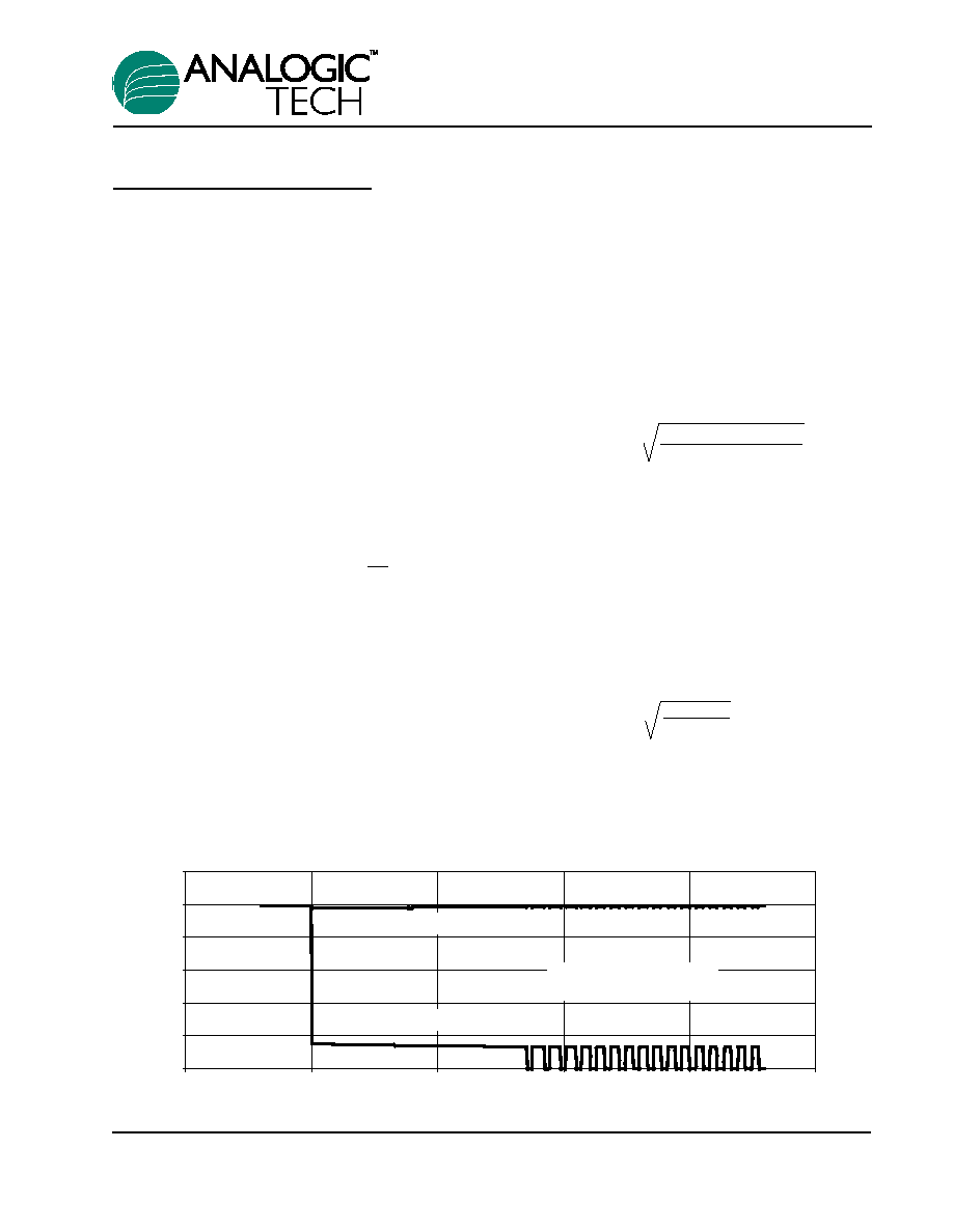
Overload Operation
0
1
2
3
4
5
6
-0.5
0
0.5
1
1.5
2
Time (s)
Voltage (V)
Output Voltage
Input Voltage
1
9 is applied to output at t = 0
R
SET
is 2 k
9

Applications Information
Input Capacitor
The input capacitor serves two purposes. First, it
protects the source power supply from transient
current effects generated by the application load
circuit. If a short circuit is suddenly applied to the
output of an AAT4601, there is a microsecond long
period during which a large can current flow before
the current limit circuitry activates. Refer to the
characteristic curve named "Short Circuit Through
0.3
." A properly sized input capacitor can dramat-
ically reduce the load switch input transient
response effects seen by the power supply and
other circuitry upstream from the AAT4601.
The second purpose of the input capacitor is to
prevent transient events generated by the load cir-
cuit from affecting the operation of the AAT4601.
For example, if an AAT4601 is used in a circuit that
operates from a 3 volt power supply with poor step
load response, it is possible that turning on the load
switch could cause the input power supply to droop
below the AAT4601's under voltage lockout thresh-
old. This drop in voltage would cause the AAT4601
to turn off until the input power supply's voltage
recovers. Since this cycle would be self-perpetuat-
ing, the entire circuit could be seen to be unstable.
In the very rare case where capacitor cost is pro-
hibitive, the output load circuit should be slew rate
limited when turned on.
Output Capacitor
In order to insure stability while the device current
limit is active, a small capacitance of approximately
1µF should be used. When the AAT4601 is activat-
ed using the ON function, there are no momentary
current transients as in the case of when a short cir-
cuit suddenly applied to a device that is already on.
Refer to the characteristic curve named "Switch
Turn-On Time." No matter how big the output
capacitor, output current is limited to the value
allowed by the threshold determined by R
SET
and
the internal current limiting circuitry. This permits
very large output capacitors to be used.
For example, USB ports are specified to have at
least 120µF of down stream capacitance from their
controlling power switch. An output capacitance as
large as 1000µF would not disturb the input power
supply to the AAT4601 used to control the USB port.
ON Input
When the AAT4601 is in the off state, the output is
an open circuit and the device quiecent current
consumption is reduced to less than 1µA. The ON
threshold voltage is set to allow the AAT4601 to be
controlled by 5 volt TTL levels as well as CMOS
power from 2.5 volts to 5 volts. The ON function
control voltage level should not exceed the input
supply level applied to the IN pin.
FAULT Output
A FAULT flag is provided to alert a system if the load
switch is not receiving a sufficient voltage level to
operate properly. If either the current limit or over
temperature circuits in any combination are active
for more than approximately two milliseconds con-
tinuously, the FAULT pin is pulled to ground inter-
nally through a 100
resistance. The 2 millisecond
delay on the FAULT function is intended to prevent
capacitive loads connected to the load switch out-
put from activating FAULT when the device is
turned on. The placement of a pull up resistor
between the FAULT pin and the IN pin is recom-
mended. Reasonable values for the pull up resistor
should range from 10k
to 100k
. Since FAULT is
an open drain terminal, it may be pulled up to any
voltage that is not greater than the level present on
the IN pin. This is done to allow the AAT4601 to sig-
nal ancillary circuitry that is powered by voltage
level less than the level on the IN pin.
Reverse Voltage
The AAT4601 is designed to control current flowing
from IN to OUT. If a voltage is applied to OUT
which is greater than that on IN, a large resulting
reverse current may flow, potentially damaging the
AAT4601.
AAT4601
1.5A Current Limited P-Channel Switch
10
4601.2001.11.0.92

AAT4601
1.5A Current Limited P-Channel Switch
4601.2001.11.0.92
11
Figure 1: AAT4601 Evaluation
Figure 2: AAT4601 Evaluation
Figure 3: AAT4601 Evaluation
board top side silk screen
board component side layout
board solder side layout
assembly drawing
Printed Circuit Board Layout
Recommendations
For proper thermal management, and to take
advantage of the low R
DS(ON)
of the AAT4601, a few
circuit board layout rules should be followed: V
IN
and V
OUT
should be routed using wider than normal
traces, and GND should be connected to a ground
plane. For best performance, C
IN
and C
OUT
should
be placed close to the package pins.
Evaluation Board Layout
The AAT4601 evaluation layout follows the printed
circuit board layout recommendations, and can be
used for good applications layout.
Note: Board layout shown is not to scale.
Ordering Information
Package Information
SOP-8
1 2
E
b
e
H
D
A1
A
A2
7 ( 4x)
c
L
y
Q
Package
Marking
Part Number
Bulk
Tape and Reel
SOP-8
AAT4601IAS-B1
AAT4601IAS-T1
TSSOP-8
AAT4601IHS-B1
AAT4601IHS-T1
AAT4601
1.5A Current Limited P-Channel Switch
12
4601.2001.11.0.92
Dim
Millimeters
Inches
Min
Max
Min
Max
A
1.35
1.75
0.053
0.069
A1
0.10
0.25
0.004
0.010
A2
1.45
0.057
B
0.33
0.51
0.013
0.020
C
0.19
0.25
0.007
0.010
D
4.80
5.00
0.189
0.197
E
3.80
4.00
0.150
0.157
e
1.27
0.050
H
5.80
6.20
0.228
0.244
L
0.40
1.27
0.016
0.050
Y
0.00
0.10
0.000
0.004
1
0∞
8∞
0∞
8∞
Note:
1. PACKAGE BODY SIZES EXCLUDE MOLD FLASH
PROTRUSIONS OR GATE BURRS.
2. TOLERANCE± 0.1000mm (4mil) UNLESS
OTHERWISE SPECIFIED
3. COPLANARITY: 0.1000mm
4. DIMENSION L IS MEASURED IN GAGE PLANE.
5. CONTROLLING DIMENSION IS MILLIMETER;
CONVERTED INCH DIMENSIONS ARE NOT
NECESSARILY EXACT.

TSSOP-8
A1
b
e
E
1 2
A
A2
E1
DETAIL A
R
L1
L
0.20
D
R1
2
E
1
DETAIL A
AAT4601
1.5A Current Limited P-Channel Switch
4601.2001.11.0.92
13
Dim
Millimeters
Inches
Min
Max
Min
Max
A
1.05
1.20
0.041
0.047
A1
0.05
0.15
0.002
0.006
A2
-
1.05
-
0.041
b
0.25
0.30
0.010
0.012
c
0.127
0.005
D-8
2.90
3.10
0.114
0.122
D-28
9.60
9.80
0.378
0.386
E
4.30
4.50
0.170
0.177
E1
6.20
6.60
0.244
0.260
e
0.65 BSC
0.025 BSC
L
0.50
0.70
0.20
0.028
L1
1.0
0.039
R
0.09
-
0.004
-
R1
0.09
-
0.004
-
1
0∞
8∞
0∞
8∞
2
12∞

This page intentionally left blank.
AAT4601
1.5A Current Limited P-Channel Switch
14
4601.2001.11.0.92
Advanced Analogic Technologies, Inc.
1250 Oakmead Parkway, Suite 310, Sunnyvale, CA 94086
Phone (408) 524-9684
Fax (408) 524-9689