 | –≠–ª–µ–∫—Ç—Ä–æ–Ω–Ω—ã–π –∫–æ–º–ø–æ–Ω–µ–Ω—Ç: AAT4610 | –°–∫–∞—á–∞—Ç—å:  PDF PDF  ZIP ZIP |
SmartSwitch
TM
General Description
The AAT4610 SmartSwitchTM is a member of
AnalogicTech's
Application
Specific
Power
MOSFETTM (ASPMTM) product family. It is a Current
Limited P-channel MOSFET power switch designed
for high-side load-switching applications. This switch
operates with inputs ranging from 2.7V to 5.5V, mak-
ing it ideal for both 3V and 5V systems. An inte-
grated current-limiting circuit protects the input sup-
ply against large currents which may cause the sup-
ply to fall out of regulation. The AAT4610 is also pro-
tected from thermal overload which limits power dis-
sipation and junction temperatures. It can be used
to control loads that require up to 1 A. Current limit
threshold is programmed with a resistor from SET to
ground. The quiescent supply current is typically a
low 15µA max. In shutdown mode, the supply cur-
rent decreases to less than 1µA.
The AAT4610 is available in a 5 pin SOT-23 spec-
ified over -40 to 85∞C.
The AAT4600 Series is a family of adjustable and
fixed SmartSwitchTM with a range of current han-
dling capabilities. Available are single versions in
adj. current limit (AAT4600, AAT4601) as well as in
fixed current limit (AAT4602, AAT4625). Dual ver-
sions (AAT4620, AAT4626) are also available.
Features
∑
2.7V to 5.5V Input voltage range
∑
Programmable over current threshold
∑
Fast transient response:
∑
<1µs response to short circuit
∑
Low quiescent current
∑
15µA typical
∑
1µA max with Switch off
∑
160m
typical R
DS(ON)
∑
Only 2.5V needed for ON/OFF Control
∑
Undervoltage Lockout
∑
Thermal shutdown
∑
Temp range -40 to 85∞C
∑
4kV ESD Rating
∑
UL Approved--File No. E217765
∑
5 pin SOT-23 package
Applications
∑
Peripheral ports
∑
Notebook computers
∑
Personal communication devices
∑
Hot swap supplies
UL Recognized Component
AAT4610
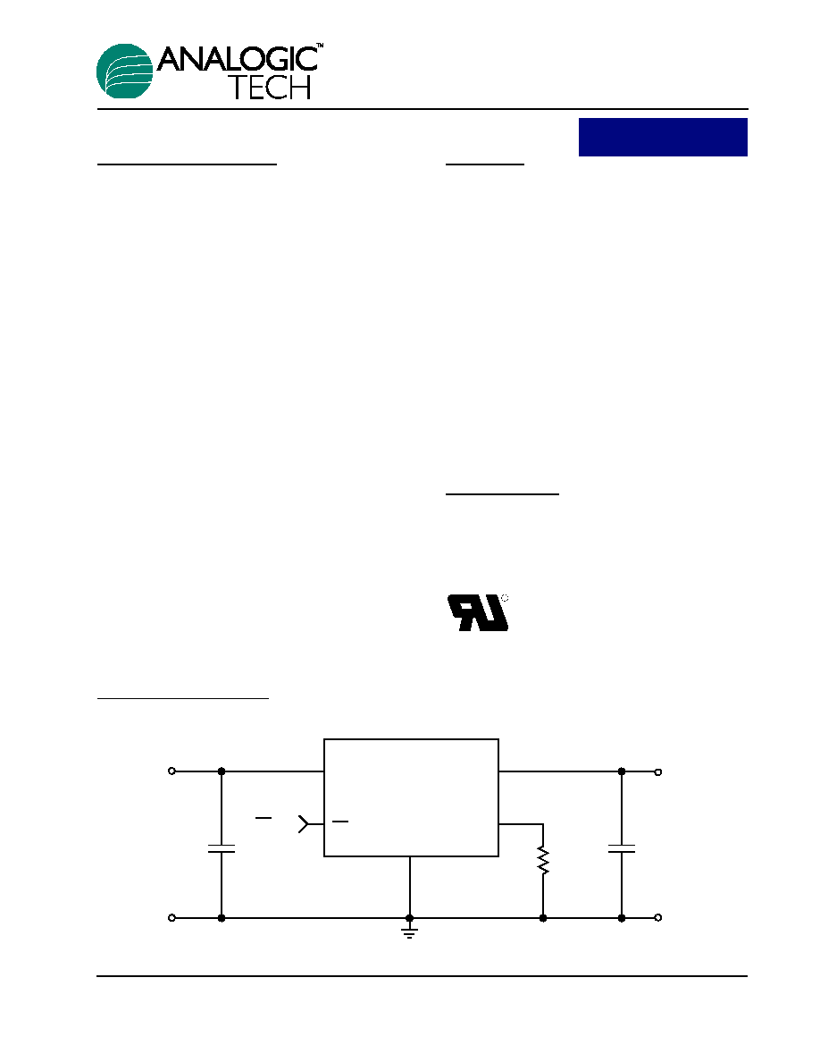
Current Limited Load Switch in SOT-23 Package
Typical Application
AAT4610
5
4
2
3
1
ON/(ON)
IN
SET
INPUT
GND
GND
GND
OUT
SOT-23
OUTPUT
ON (ON)
0.47
µ
F
R
SET
1
µ
F
Preliminary
Information
4610.2001.9.0.97
1

AAT4610
Current Limited Load Switch in SOT-23 Package
2
4610.2001.9.0.97
Pin Configuration
5-Pin SOT-23
(Top View)
Pin Descriptions
Pin #
Symbol
Function
1
OUT
P-channel MOSFET drain. Connect 0.47µF capacitor from OUT to GND.
2
GND
Ground connection
3
SET
Current-Limit Set Input. A resistor from SET to ground sets the current limit for
the switch.
4
ON
Enable Input. Two versions are available, active-high and active-low. See order-
ing information for details.
5
IN
P-channel MOSFET source. Connect 1µF capacitor from IN to GND.
1
2
3
SET
OUT
4
5
GND
IN
ON

AAT4610
Current Limited Load Switch in SOT-23 Package
4610.2001.9.0.97
3
Absolute Maximum Ratings
(T
A
=25∞C unless otherwise noted)
Note: Stresses above those listed in Absolute Maximum Ratings may cause permanent damage to the device. Functional operation at con-
ditions other than the operating conditions specified is not implied. Only one Absolute Maximum rating should be applied at any one time.
Note 1: Human body model is a 100pF capacitor discharged through a 1.5k
resistor into each pin.
Thermal Characteristics
Note 2: Mounted on a demo board.
Electrical Characteristics
(V
IN
= 5V, T
A
= -40 to 85∞C unless otherwise noted. Typical values
are at T
A
=25∞C)
Symbol
Description
Conditions
Min
Typ
Max
Units
V
IN
Operation Voltage
2.7
5.5
V
I
Q
Quiescent Current
V
IN
= 5V, ON (ON) = active, I
OUT
= 0
15
30
µ
A
I
Q(OFF)
Off Supply Current
ON (ON) =inactive, V
IN
= 5.5V
1
µ
A
I
SD(OFF)
Off Switch Current
ON (ON) = inactive, V
IN
= 5.5V, V
OUT
= 0
.03
15
µ
A
V
UVLO
Undervoltage Lockout
Rising edge, 1% hysteresis,
2.0
2.3
2.7
V
V
IN
=5.0V
160
180
m
R
DS(ON)
On-Resistance
V
IN
=4.5V
165
m
V
IN
=3.0V
195
230
m
I
LIM
Current Limit
R
SET
= 6.8k
.75
1
1.25
A
I
LIM(MIN)
Minimum Current Limit
150
mA
V
ON(L)
ON (ON) Input Low Voltage
0.8
V
V
ON(H)
ON (ON) Input High Voltage
V
IN
=2.7V to 3.6V
2.0
V
V
IN
=4.5V to 5.5V
2.4
V
I
ON(SINK)
ON (ON) Input leakage
V
ON
= 5.5V
0.01
1
µ
A
T
RESP
Current Limit Response Time
V
IN
=5V
0.8
µ
s
T
OFF
Turn-Off Time
V
IN
=5V, R
L
=10
0.4
2
µ
s
T
ON
Turn-On Time
V
IN
=5V, R
L
=10
40
200
µ
s
Symbol
Description
Value
Units
JA
Thermal Resistance
2
150
∞C/W
P
D
Power Dissipation
2
667
mW
Symbol
Description
Value
Units
V
IN
IN to GND
-0.3 to 6
V
V
ON
ON(ON) to GND
-0.3 to V
IN
+0.3
V
V
SET,
V
OUT
SET, OUT to GND
-0.3 to V
IN
+0.3
V
I
MAX
Maximum Continuous Switch Current
2
A
T
J
Operating Junction Temperature Range
-40 to 150
∞C
T
LEAD
Maximum Soldering Temperature (at Leads)
300
∞C
V
ESD
ESD Rating
1
- HBM
4000
V

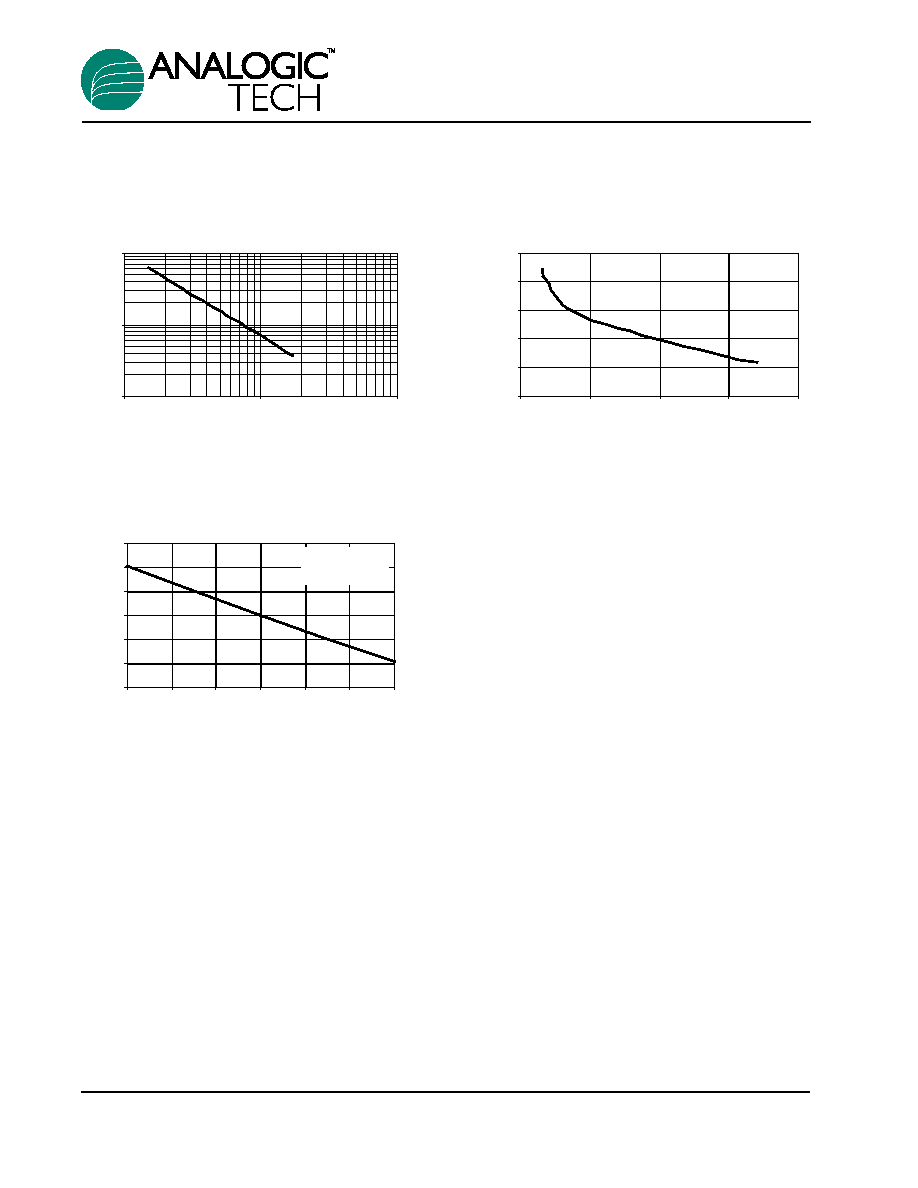
Typical Characteristics
(Unless otherwise noted, V
IN
= 5V, T
A
= 25∞C)
Off-Switch Current vs. Temperature
Temperature (C )
Off-Switch
Current
(
µ
A)
0.001
0.01
0.1
1
10
-40
-20
0
20
40
60
80
100
120
Off-Supply Current vs. Temperature
0.01
0.1
1
10
-40
-20
0
20
40
60
80
100
120
Temperature (C )
Off-Supply
C
urrent
(
µ
A)
R
DS(ON)
vs. Temperature
0
50
100
150
200
250
-40
-20
0
20
40
60
80
100
Te
R
DS(ON)
(m
)
mperature (C)
Input = 3 V
Input = 5 V
Output Current vs
V
OUT
0
0.2
0.4
0.6
0
1
2
3
4
5
Vout ( V )
Output
Current
(A)
R
SET
=16 k
Quiescent Current
0
10
20
30
40
2.5
3
3.5
4
4.5
5
5.5
Input ( V )
Input (
µ
A
)
Quiescent Current vs. Temperature
0
5
10
15
20
25
-40
-20
0
20
40
60
80
100
120
Temperature
Quiescent Current (
µ
A)
(C)
AAT4610
Current Limited Load Switch in SOT-23 Package
4
4610.2001.9.0.97

(Unless otherwise noted, V
IN
= 5V, T
A
= 25∞C)
Short Circuit through 0.6
0
2
4
6
8
0
1
2
3
Time (
µ
s)
Input
and
Output
-3
0
3
6
9
Output (A)
Output Current
Input Voltage
Output Voltage
(V)
Short Circuit through 0.3
0
2
4
6
8
0
1
2
3
Time (
µ
s)
Input
and
Output
-4
0
4
8
12
Output (A)
Output Current
Input Voltage
Output Voltage
(V)
-1
0
1
2
3
4
5
6
- 0.5
0
0.5
1
Time (
µ
s)
Voltage
(
V
)
Output
ON
I
OUT
=I
LI MIT
Turn-Off
R
L
= 10
Turn-On
R
L
= 10
, C
L
= 0.47
µ
F
-1
0
1
2
3
4
5
6
- 20
0
20
40
60
Time (
µ
s)
Voltage
(
V
)
Output
ON
I
OUT
=I
LIM IT
Turn-OFF vs. Temperature
0
0.05
0.1
0.15
0.2
0.25
0.3
0.35
0.4
0.45
- 40
- 20
0
20
40
60
80
100
Temperature (C )
Turn-OFF
Time
(
µ
s)
Vin = 3V
Vin = 5V
Turn-ON vs. Temperature
0
10
20
30
40
50
60
70
80
- 40
- 20
0
20
40
60
80
100
Temperature ( C )
Turn-ON
Time
(
µ
s)
Vin=5V
Vin=3V
AAT4610
Current Limited Load Switch in SOT-23 Package
4610.2001.9.0.97
5
(Unless otherwise noted, V
IN
= 5V, T
A
= 25∞C)
Current Limit v. Temperature
-6%
-4%
-2%
0%
2%
4%
6%
-50
- 25
0
25
50
75
100
Temperature (C)
Current
Limit
(
%)
R
SET
= 22.1k
V
IN
-V
OUT
=0.5V
R
SET
coefficent vs I
LIM
5
6
7
8
9
10
0
0.5
1
1.5
2
I
LIM
(A)
R
SET
I
LIM
Product
(
k
V
)
R
SET
vs I
LIM
1
10
100
0.1
10
1
I
LIM
(A)
R
SET
(k
)
AAT4610
Current Limited Load Switch in SOT-23 Package
6
4610.2001.9.0.97
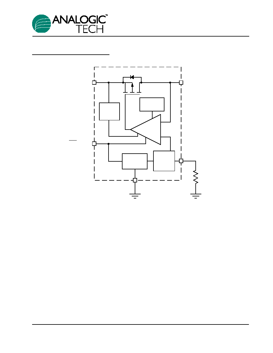
Functional Block Diagram
Current
Limit
1.2V
Reference
Under-
voltage
Lockout
Over-Temp
Protection
OUT
SET
GND
R
SET
ON (ON)
IN
AAT4610
Current Limited Load Switch in SOT-23 Package
4610.2001.9.0.97
7
Applications Information
Setting Current Limit
In most applications, the variation in I
LIM
must be
taken into account when determining R
SET.
The I
LIM
variation is due to processing variations from part
to part, as well as variations in the voltages at IN
(pin 5) and OUT (pin 3), plus the operating temper-
ature. See charts "Current Limit vs. Temperature",
and "Output Current vs. V
OUT
". Together these
three factors add up to a ±25% tolerance (see I
LIM
specification in Electrical Characteristics section).
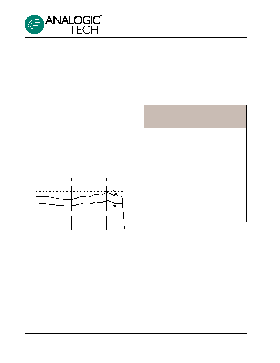
In the figure below, a cold device with a statistical-
ly higher current limit, and a hot device with a sta-
tistically lower current limit, both with R
SET
equal to
10.5k
are shown. While the chart, "R
SET
vs. I
LIM
"
indicates an I
LIM
of 0.7A with an R
SET
of 10.5k
,
this figure shows that the actual current limit will be
at least 0.525A, and no greater than 0.880A.
To determine R
SET,
start with the maximum current
drawn by the load, and multiply it by 1.33. (typi-
cal_I
LIM
= minimum_I
LIM
/ 0.75) This is the typical
current limit value. Next, refer to "R
SET
vs. I
LIM
" and
find the R
SET
that corresponds to the typical current
limit value. Choose the largest resistor available
that is less than or equal to it. For greater precision,
the value of R
SET
may also be calculated using the
I
LIM
R
SET
product found in the chart "R
SET
coeffi-
cient vs. I
LIM
". The maximum current is derived by
multiplying the typical current for the chosen R
SET
in the chart by 1.25. A few standard resistor values
are listed in the table "Current Limit R
SET
Values".
Current Limit R
SET
Values
Example: A USB port requires 0.5A. 0.5A multiplied
by 1.33 is 0.665A. From the chart named "R
SET
vs.
I
LIM
", R
SET
should be less than 11k
. 10.5 k
is a
standard value that is a little less than 11k
but
very close. The chart reads approximately 0.700A
as a typical I
LIM
value for 10.5k
. Multiplying
0.700A by 0.75 and 1.25 shows that the AAT4610
will limit the load current to greater than 0.525A but
less than 0.875A.
Current Limit Using 10.5 k
0
0.2
0.4
0.6
0.8
1
1.2
0
1
2
3
4
5
Vout ( V )
I
LIM
(A
)
0.88 A
0.525 A
Device with high current limit at -40 C
Device with low current limit at 85 C
AAT4610
Current Limited Load Switch in SOT-23 Package
8
4610.2001.9.0.97
R
SET
Current
Device will
Device always
(k
)
Limit typ not current
current limits
(mA)
limit below:
below:
(mA)
(mA)
40.2
200
150
250
30.9
250
188
313
24.9
300
225
375
22.1
350
263
438
19.6
400
300
500
17.8
450
338
563
16.2
500
375
625
14.7
550
413
688
13.0
600
450
750
10.5
700
525
875
8.87
800
600
1000
7.50
900
675
1125
6.81
1000
750
1250
6.04
1100
825
1375
5.49
1200
900
1500
4.99
1300
975
1625
4.64
1400
1050
1750

Operation in Current Limit
When a heavy load is applied to the output of the
AAT4610, the load current is limited to the value of
I
LIM
determined by R
SET
. See the figure "Overload
Operation". Since the load is demanding more cur-
rent than I
LIM
, the voltage at the output drops. This
causes the AAT4610 to dissipate a larger than nor-
mal quantity of power, and its die temperature to
increase. When the die temperature exceeds an
over temperature limit, the AAT4610 will shut down
until is has cooled sufficiently, at which point it will
startup again. The AAT4610 will continue to cycle
on and off until the load is removed, power is
removed, or until a logic high level is applied to ON
(pin 4).
Enable Input
In many systems, power planes are controlled by
integrated circuits which run at lower voltages than
the power plane itself. The enable input ON (pin 4)
of the AAT4610 has low and high threshold volt-
ages that accommodate this condition. The thresh-
old voltages are compatible with 5 volt TTL, and 2.5
volt to 5 volt CMOS.
Reverse Voltage
The AAT4610 is designed to control current flowing
from IN to OUT. If a voltage is applied to OUT which
is greater than the voltage on IN, large currents may
flow. This could cause damage to the AAT4610.
AAT4610
Current Limited Load Switch in SOT-23 Package
4610.2001.9.0.97
9
Overload Operation
0
1
2
3
4
5
-0.05
0
0.05
0.1
0.15
0.2
0.25
0.3
Tim e ( s )
Outpu
t ( V
)
0
0.25
0.5
0.75
1
Output (A)
Output Current
Output Voltage
1
load is turned on at time = 0
Ordering Information
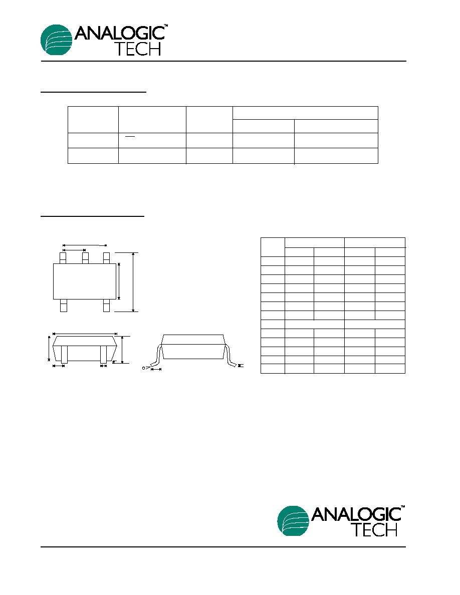
Package Information
SOT-23-5
E
A
A1
c
b
D
e
S1
L
I
H
S
Package
Enable
Marking
Part Number
Bulk
Tape and Reel
SOT-23-5
ON (active low)
N/A
AAT4610IGV-T1
SOT-23-5
ON (active high)
N/A
AAT4610IGV-1-T1
AAT4610
Current Limited Load Switch in SOT-23 Package
Dim
Millimeters
Inches
Min
Max
Min
Max
A
0.95
1.45
0.037
0.057
A1
0.05
0.15
0.002
0.006
A2
0.90
1.30
0.035
0.051
b
0.35
0.50
0.014
0.019
c
0.08
0.20
0.003
0.078
D
2.84
3.00
0.112
0.112
E1.50
1.70
0.059
0.067
e
1.90
0.0748
H
2.60
3.00
0.102
0.118
L
0.35
0.55
.0137
.0216
S
0.47
0.55
0.019
.0216
S1
.95
0.037
0∞
10∞
0∞
10∞
10
4610.2001.9.0.97
Advanced Analogic Technologies, Inc.
1250 Oakmead Parkway, Suite 310, Sunnyvale, CA 94086
Phone (408) 524-9684
Fax (408) 524-9689