
SmartSwitch
TM
AAT4618
Current Limited Load Switch
Preliminary
Information
4618.2002.2.0.9
1
General Description
The AAT4618 SmartSwitchTM is a member of
AnalogicTech's Application Specific Power MOS-
FETTM (ASPMTM) product family. It is a Current
Limited P-channel MOSFET power switch designed
for high-side load-switching applications operating
with inputs ranging from 2.4V to 5.5V which makes it
ideal for 2.5V, 3V and 5V systems. An integrated cur-
rent-limiting circuit protects the input supply from large
currents which potentially cause the supply to fall out
of regulation. In addition, the AAT4618 thermal over-
load protection limits power dissipation and junction
temperatures associated with prolonged periods of
operation in current limit. Due to its low R
DS(ON)
, the
AAT4618 can be used to control loads that require up
to 500mA even while operating at high ambient tem-
peratures. The ultra fast current-limit response to a
sudden short circuit is a mere 400ns which reduces
the requirements of local supply bypassing. An open
drain FAULT flag signals an over current or over tem-
perature condition after a 4ms timeout. Quiescent
current is a low 10µA and in shutdown mode, the sup-
ply current decreases to less than 1µA.
The AAT4618 is available in a 5 pin SOT-23, and an
8 pin SC70JW specified over a -40 to 85∞C temper-
ature range.
The AAT4600 Series is a family of adjustable and
fixed SmartSwitchTM products with a range of current
handling capabilities. Available are single versions
with adjustable current limit (AAT4610, AAT4601) as
well as fixed current limit (AAT4625), and dual ver-
sions with fixed current limit (AAT4626, AAT4670).
Features
∑
2.4V to 5.5V Input voltage range
∑
500mA min current limit trip threshold
∑
Fast transient response:
∑
400ns response to short circuit
∑
Low quiescent current
∑
10µA typical
∑
< 1µA with Switch off
∑
125m
typical R
DS(ON)
∑
FAULT flag with 4ms blanking
∑
Undervoltage Lockout
∑
Thermal shutdown
∑
Temp range -40 to 85∞C
∑
4kV ESD Rating
∑
5 pin SOT23 package
∑
8 pin SC70JW package
Applications
∑
Peripheral ports
∑
USB Ports
∑
Notebook computers
∑
Personal communication devices
∑
Hot swap supplies
Typical Application
AAT4618
ON (ON)
IN
OUT
FAULT
GND
ON
(ON)
100k
INPUT
GND
GND
C
IN
1
µ
F
C
OUT
0.47
µ
F
OUTPUT
FAULT

AAT4618
Current Limited Load Switch
2
4618.2002.2.0.9
Pin Descriptions
Pin Configuration
SOT23-5
SC70JW-8
ON (ON)
IN
IN
1
2
GND
GND
GND
OUT
FAULT
1
2
3
4
8
7
6
5
1
2
3
ON (ON)
FAULT
IN
4
5
GND
OUT
Pin #
SOT23-5
SC70JW-8
Symbol
Function
1
5
OUT
P-channel MOSFET drain
2
6, 7, 8
GND
Ground connection
3
1
FAULT
Open-drain FAULT output
4
2
ON (ON)
Enable Input: 4618 active low, 4618-1 active high
5
3, 4
IN
P-channel MOSFET source

AAT4618
Current Limited Load Switch
4618.2002.2.0.9
3
Absolute Maximum Ratings
(T
A
=25∞C unless otherwise noted)
Note: Stresses above those listed in Absolute Maximum Ratings may cause permanent damage to the device. Functional operation at con-
ditions other than the operating conditions specified is not implied. Only one Absolute Maximum rating should be applied at any one time.
Note 1: Human body model is a 100pF capacitor discharged through a 1.5k
resistor into each pin.
Thermal Characteristics
Note 2: Mounted on a demo board.
Electrical Characteristics
(V
IN
= 5V, T
A
= -40 to 85∞C unless otherwise noted. Typical values
are at T
A
=25∞C; bold values denote full temperature range)
Note 3: For V
IN
outside this range consult Typical ON (ON) Threshold curve.
Symbol
Description
Conditions
Min
Typ
Max
Units
V
IN
Operation Voltage
2.4
5.5
V
I
Q
Quiescent Current
V
IN
= 5V, ON (ON) = active, I
OUT
= 0
10
20
µA
I
Q(OFF)
Off Supply Current
ON (ON) = inactive, V
IN
= 5.5V
1
µA
I
SD(OFF)
Off Switch Current
ON (ON) = inactive, V
IN
= 5.5V, V
OUT
= 0
0.1
1
µA
V
UVLO
Undervoltage Lockout
V
IN
falling
1.9
V
V
UVLO(hys)
Undervoltage Lockout Hysteresis
0.3
V
R
DS(ON)
On-Resistance
V
IN
= 5.0V, T
A
= 25∞C
125
175
m
V
IN
= 3.0V, T
A
= 25∞C
155
225
TC
RDS
ON-Resistance Temp-co
2800
ppm/∞C
I
LIM
Current Limit
V
OUT
= V
IN
- 0.5V
500
750
1000
mA
V
ON(L)
ON (ON) Input Low Voltage
V
IN
= 2.7V to 5.5V
3
0.8
V
V
ON(H)
ON (ON) Input High Voltage
V
IN
= 2.7V to
4.2V
3
2.0
V
V
IN
= > 4.2V to 5.0V
3
2.4
V
I
ON(SINK)
ON (ON) Input leakage
V
ON (ON)
= 5.5V
0.01
1
µA
t
RESP
Current Loop Response
V
IN
= 5V
400
ns
T
OFF
Turn-Off Time
V
IN
= 5V, R
L
= 20
5
µs
T
ON
Turn-On Time
V
IN
= 5V, R
L
= 20
1
µs
V
FAULTLOW
FAULT Logic Output Low
I
SINK
= 1mA
0.4
V
I
SINK
FAULT Logic Output High
V
FAULT
= 5.5V
0.5
1
µA
Leakage Current
T
blank
Fault Blanking Time
4
ms
T
SD
Over-temperature threshold
V
IN
= 5V
125
∞C
Symbol
Description
Value
Units
JA
Maximum Thermal Resistance
2
150
∞C/W
P
D
Maximum Power Dissipation
2
667
mW
Symbol
Description
Value
Units
V
IN, FAULT
IN, FAULT to GND
-0.3 to 6
V
V
ON
ON (ON) to GND
-0.3 to V
IN
+1
V
V
OUT
OUT to GND
-0.3 to V
IN
+0.3
V
I
OUT
Output Current
Internally Limited
A
T
J
Operating Junction Temperature Range
-40 to 150
∞C
V
ESD
ESD Rating
1
--HBM
4000
V
T
LEAD
Maximum Soldering Temperature (at Leads)
300
∞C
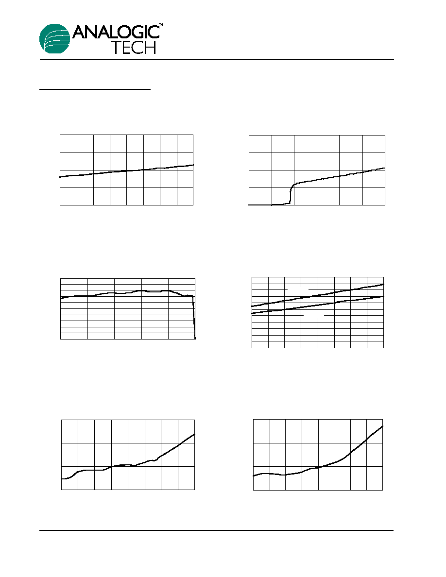
Typical Characteristics
(Unless otherwise noted, V
IN
= 5V, T
A
= 25∫C)
Off-Switch Current vs. Temperature
0.00
0.01
0.10
1.00
-40
-20
0
20
40
60
80
100
120
Temperature (
∞
C)
Off-Switch Current (
µ
A)
Off-Supply Current vs. Temperature
0.00
0.01
0.10
1.00
-40
-20
0
20
40
60
80
100
120
Temperature (
∞
C)
Off-Supply Current (
µ
A)
R
DS(ON)
vs. Temperature
0
20
40
60
80
100
120
140
160
180
200
220
-40
-20
0
20
40
60
80
100
120
Temperature (
∞
C)
R
DS(ON)
(m
)
V
IN
=3V
V
IN
=5V
Current Limit vs. V
OUT
0.0
0.1
0.2
0.3
0.4
0.5
0.6
0.7
0.8
0.9
1.0
0
1
2
3
4
5
V
OUT
(V)
Current Limit (A)
Quiescent Current vs. Input Voltage
0
5
10
15
20
0
1
2
3
4
5
6
IN (V)
Quiescent Current (
µ
A)
Quiescent Current vs. Temperature
0
5
10
15
20
-40
-20
0
20
40
60
80
100
120
Temperature (
∞
C)
Quiescent Current (
µ
A)
AAT4618
Current Limited Load Switch
4
4618.2002.2.0.9
AAT4618
Current Limited Load Switch
4618.2002.2.0.9
5
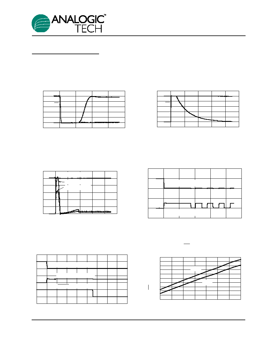
Typical Characteristics
(Unless otherwise noted, V
IN
= 5V, T
A
= 25∫C)
ON (ON) Threshold vs. V
IN
0.4
0.6
0.8
1
1.2
1.4
1.6
1.8
2
2.2
2.4
2
2.5
3
3.5
4
4.5
5
5.5
V
IN
(V)
ON (ON) Threshold (V)
V
ON(H)
V
ON(L)
Fault Delay from Short Circuit
Time (1ms/div)
Output Voltage (5V/div)
Output Current (1A/div)
FAULT (5V/div)
Thermal Shutdown Response
Time (50ms/div)
Output Voltage (5V/div)
Output Current (1A/div)
Short Circuit through 0.3
0
1
2
3
4
5
6
-1
0
1
2
3
4
5
Time (
µ
s)
Input and Output (V)
0
2
4
6
8
10
12
Output (A)
Output Current
Output Voltage
Input Voltage
Turn-Off
R
L
=20
, C
L
=0.47
µ
F
-1
0
1
2
3
4
5
6
-10
0
10
20
30
40
50
Time (
µ
s)
Voltage (V)
ON
OUT
Turn-On
R
L
=20
, C
L
=0.47
µ
F
-1
0
1
2
3
4
5
6
-0.5
0.0
0.5
1.0
1.5
2.0
Time (
µ
s)
Voltage (V)
ON
OUT

Functional Block Diagram
IN
OUT
ON (ON)
GND
Under-Voltage
Lockout
Over-Temp
Protection
Current
Limit
FAULT
4ms Delay
AAT4618
Current Limited Load Switch
6
4618.2002.2.0.9
Functional Description
The AAT4618 is a single channel current limited
load switch that protects against short circuits by
current limiting to a preset level. A patented fast
acting current limit loop limits the current in a frac-
tion of a micro second and instantly resets to low
impedance once the short circuit condition is
removed. The AAT4618 is internally protected
from thermal damage by an over temperature
detection circuit. If the die temperature reaches
the internal thermal limit, the power device is
switched off until the die temperature cools to a
level below the thermal limit threshold. The device
will thermal cycle indefinitely until the over current
condition is removed. The AAT4618 operates with
input voltages ranging from 2.4V to 5.5V which,
along with its extremely low operating current,
makes it ideal for battery-powered applications. In
cases where the input voltage drops below 2.4V,
the AAT4618 MOSFET is protected from entering
the saturated region of operation by being auto-
matically shut down by an under voltage lockout
circuit. A current limit condition is reported by the
open drain FAULT output. A four millisecond blank-
ing interval prevents false reporting during the
charging of a capacitive load, which typically
occurs during device turn-on, but may also occur
during a port hot plug-in event.
The AAT4618 is ideally suited for protection of
peripheral ports such as USB, RS232 and parallel
ports.

Applications Information
Input Capacitor
The input capacitor, C
IN
protects the power supply
from current transients generated by the load
attached to the AAT4618. When a short circuit is
suddenly applied to the output of the AAT4618, a
large current, limited only by the R
DS(ON)
of the
MOSFET, will flow for less than 1µs before the cur-
rent limit circuitry activates. (See characteristic
curve "Short Circuit Through 0.3
.") In this event,
a moderately sized C
IN
will dramatically reduce the
voltage transient seen by the power supply and by
other circuitry upstream from the AAT4618. The
extremely fast short circuit response time of the
AAT4618 reduces the size requirement of C
IN
.
C
IN
should be located as close to the device VIN pin
as practically possible. Ceramic, tantalum or alu-
minum electrolytic capacitors are appropriate for
C
IN
. There is no specific capacitor ESR requirement
for C
IN
. However, for higher current operation,
ceramic capacitors are recommended for C
IN
due to
their inherent capability over tantalum capacitors to
withstand input current surges from low impedance
sources such as batteries in portable devices.
Output Capacitor
In order to insure stability while current limit is
active, a small capacitance of approximately
0.47µF is required. No matter how large the output
capacitor however, output current is limited to the
value set by the AAT4618 current limiting circuitry,
so very large output capacitors can be used.
For example, USB ports are specified to have at
least 120µF of capacitance down stream from their
controlling power switch. The current limiting circuit
will allow an output capacitance of 1000µF or more
without disturbing the upstream power supply.
ON (Enable Input)
In many systems, power planes are controlled by
integrated circuits which run at lower voltages than
the power plane itself. The enable input (ON) of
the AAT4618 has low and high threshold voltages
that accommodate this condition. The threshold
voltages are compatible with 5 volt TTL, and 2.5
volt to 5 volt CMOS systems.
When switching the AAT4618 on into a capacitive
load, the AAT4618 will charge the output capacitive
load at a rate no greater than the current limit setting.
Attaching Loads
Capacitive loads attached to an enabled AAT4618
will charge at a rate no greater than the current limit
setting.
FAULT Output
The FAULT flag is provided to alert the system if an
AAT4618 load is not receiving sufficient voltage to
operate properly. If current limit or over tempera-
ture circuits in any combination are active for more
than approximately four milliseconds, the FAULT
flag is pulled to ground through approximately
100
. The filtering of voltage or current transients
of less than four milliseconds prevents capacitive
loads connected to the AAT4618 output from acti-
vating the FAULT flag when they are initially
attached. Pull up resistances of 1k
to 100k
are
recommended. Since FAULT is an open drain ter-
minal, it may be pulled up to any unrelated voltage
less than the maximum operating voltage of 5.5V,
allowing for level shifting between circuits.
Thermal Considerations
Since the AAT4618 has internal current limit and
over temperature protection, junction temperature
is rarely a concern. However, if the application
requires large currents in a hot environment, it is
possible that temperature rather than current limit
will be the dominant regulating condition. In these
applications, the maximum current available with-
out risk of an over temperature condition must be
calculated. The maximum internal temperature
while current limit is not active can be calculated
using Equation 1.
T
J
(MAX) = I
MAX
2
◊
R
DS(ON)
(MAX)
◊
R
JA
+ T
A
(MAX)
In Equation 1, I
MAX
is the maximum current
required by the load. R
DS(ON)
(MAX) is the maxi-
mum rated R
DS(ON)
of the AAT4618 at high temper-
ature. R
JA
is the thermal resistance between the
AAT4618 die and the board onto which it is mount-
ed. T
A
(MAX) is the maximum temperature that the
PCB under the AAT4618 would be if the AAT4618
were not dissipating power. Equation 1 can be
rearranged to solve for I
MAX
; Equation 2.
I
MAX
=
T
SD
(MIN) - T
A
(MAX)
R
DS(ON)
(MAX)
◊
R
JA
AAT4618
Current Limited Load Switch
4618.2002.2.0.9
7

T
SD
(MIN) is the minimum temperature required to
activate the AAT4618 over temperature protection.
With typical specification of 125∞C, 115∞C is a safe
minimum value to use.
For example, if an application is specified to oper-
ate in 50∞C environments, the PCB operates at
temperatures as high as 85∞C. The application is
sealed and its PCB is small, causing R
JA
to be
approximately 150 ∞C/W. Using Equation 2,
I
MAX
=
115 - 85
= 950 mA
220m
◊
150
The AAT4618 is safe to operate at the minimum
current limit level of 500mA at 85∞C.
AAT4618
Current Limited Load Switch
8
4618.2002.2.0.9

Ordering Information
Package Information
SOT23-5
E
A
A1
c
b
D
e
S1
L
I
H
S
Package
Enable
Marking
Part Number
Bulk
Tape and Reel
SOT23-5
Active Low
N/A
AAT4618IGV-T1
SOT23-5
Active High
N/A
AAT4618IGV-1-T1
SC70JW-8
Active Low
N/A
AAT4618IJS-T1
SC70JW-8
Active High
N/A
AAT4618IJS-1-T1
AAT4618
Current Limited Load Switch
4618.2002.2.0.9
9
Dim
Millimeters
Inches
Min
Max
Min
Max
A
0.95
1.45
0.037
0.057
A1
0.05
0.15
0.002
0.006
A2
0.90
1.30
0.035
0.051
b
0.35
0.50
0.014
0.019
c
0.08
0.20
0.003
0.078
D
2.84
3.00
0.112
0.112
E
1.50
1.70
0.059
0.067
e
1.90
0.0748
H
2.60
3.00
0.102
0.118
L
0.35
0.55
.0137
.0216
S
0.47
0.55
0.019
.0216
S1
.95
0.037
0∞
10∞
0∞
10∞

SC70JW-8
1
D
A
A2
b
E
e
e
e
L
E1
A1
c
0.048REF
AAT4618
Current Limited Load Switch
10
4618.2002.2.0.9
Advanced Analogic Technologies, Inc.
1250 Oakmead Parkway, Suite 310, Sunnyvale, CA 94086
Phone (408) 524-9684
Fax (408) 524-9689
Dim
Millimeters
Inches
Min
Max
Min
Max
E
2.10 BSC
0.083 BSC
E1
1.75
2.00
0.069
0.079
L
0.23
0.40
0.009
0.016
A
1.10
0.043
A1
0
0.10
0.004
A2
0.70
1.00
0.028
0.039
D
2.00 BSC
0.079 BSC
e
0.50 BSC
0.020 BSC
b
0.15
0.30
0.006
0.012
c
0.10
0.20
0.004
0.008
0
8∫
0
8∫
1
4∫
10∫
4∫
10∫