SmartSwitch
TM
General Description
The AAT4626
SmartSwitchTM
is
part
of
AnalogicTech's
Application
Specific
Power
MOSFETTM (ASPMTM) product family. It is a dual-
channel 500mA current-limited P-channel MOSFET
power switch designed for high-side load-switching
applications. This switch operates with inputs rang-
ing from 2.7V to 5.5V, making it ideal for both 3V
and 5V systems. An integrated current-limiting cir-
cuit protects the input supply against large changes
in load current which may cause the supply to fall
out of regulation. The AAT4626 is also protected
from thermal overload which limits power dissipa-
tion and junction temperatures. The current limit
threshold is factory programmed at 1.0A, with a
maximum of 1.5A. The quiescent supply current is
typically a low 20µA. In shutdown mode, the supply
current decreases to less than 1µA.
The AAT4626 is available in 8 pin SOP or TSSOP
specified over a -40 to 85∞C temperature range.
The AAT4600 Series is a family of adjustable and
fixed SmartSwitchTM products with a range of cur-
rent handling capabilities. Single versions with
adjustable current limit (AAT4601) or fixed current
limit (AAT4625) as well as dual versions with fixed
current limit (AAT4626) are also available.
Features
∑
Compliant to USB 1.1 and 2.0 specifications
∑
2.7V to 5.5V Input voltage range
∑
500mA (min) continuous current per channel
∑
1.25A (max) current limit per channel
∑
90m
typical R
DS(ON)
∑
Low quiescent current
∑
Typically 20µA
∑
1µA max with Switches off
∑
Thermal shutdown
∑
Slew rate limited turn on
∑
Fault flag with 2ms blanking
∑
Undervoltage Lockout
∑
Temp range -40 to 85∞C
∑
UL Approved--File No. E217765
∑
8 pin SOP or TSSOP package
Applications
∑
USB ports and peripherals
∑
Notebook computers
∑
Hot swap supplies
∑
General purpose power switching
UL Recognized Component
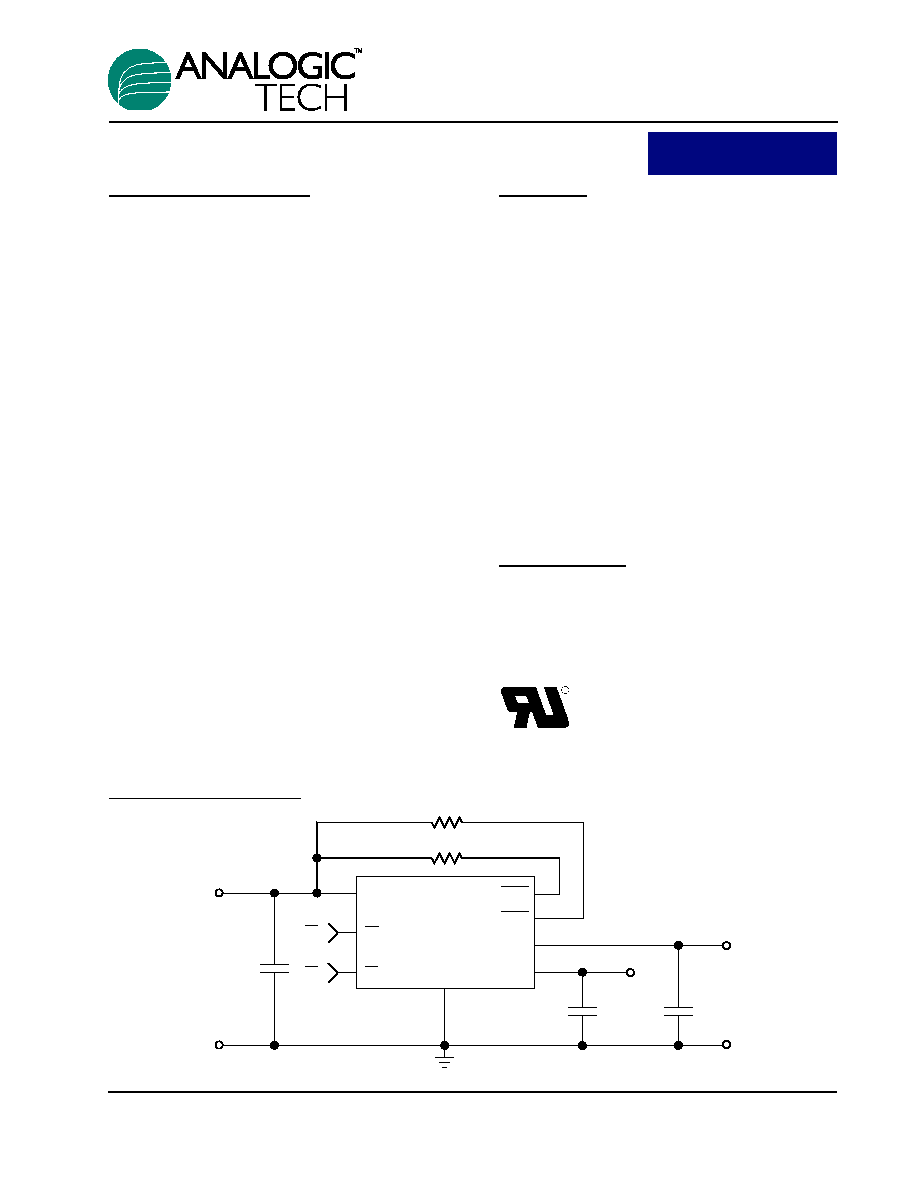
AAT4626
USB Dual-Channel Power Switch
Typical Application
AAT4626
V
CC
5.0V
GND
GND
47
µ
F
47
µ
F
FLGA
FLGB
OUTA
OUTB
(ENB)
ENB
(ENB)
ENB
(ENA)
ENA
(ENA)
ENA
OUTPUTB
OUTPUTA
0.1
µ
F
100k
100k
1
4
8
5
2
6
3
Preliminary
Information
4626.2002.1.0.93
1
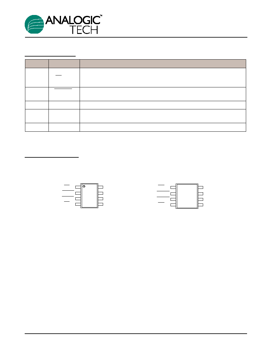
Pin Descriptions
Pin Configuration
SOP-8
TSSOP-8
(Top View)
(Top View)
1
2
IN
OUTA
GND
OUTB
ENA (ENA)
FLGA
FLGB
ENB (ENB)
1
2
3
4
8
7
6
5
1
2
ENA (ENA)
ENB (ENB)
FLGA
FLGB
OUTA
IN
GND
OUTB
Pin #
Symbol
Function
1 / 4
EN(A/B)Enable Inputs: Logic-compatible enable input. High input > 2.1V typical. Low
(EN(A/B))
input < 1.9V typical. Active high or active low option available; see Ordering
Information for details.
2 / 3
FLG(A/B)Fault Flag Outputs: Active-low, open-drain output. Indicates over current,
UVLO and thermal shutdown.
6
GND
Ground connection
7
IN
Supply Input: This pin is the P-channel MOSFETs' source connections. Also
supplies the IC's internal circuitry.
8 / 5
OUT(A/B)Switch Outputs: These pins are the P-channel MOSFET drain connection.
AAT4626
USB Dual-Channel Power Switch
2
4626.2002.1.0.93

Absolute Maximum Ratings
(T
A
=25∞C unless otherwise noted)
Note: Stresses above those listed in Absolute Maximum Ratings may cause permanent damage to the device. Functional operation at con-
ditions other than the operating conditions specified is not implied. Only one Absolute Maximum rating should be applied at any one time.
Thermal Information
Note 1: Mounted on an FR4 printed circuit board with 1 oz. copper ground plane.
Electrical Characteristics
(V
IN
= 5V, T
A
= -40 to 85∞C unless otherwise noted. Typical values
are at T
A
=25∞C; bold values designate full temperature range)
Symbol
Description
Conditions
Min
Typ
Max
Units
I
q
Quiescent Current
V
IN
=5V, ENA and ENB active
20
40
µA
V
IN-THRSH
Enable Input Threshold
Low-to-high transition
2.4
V
High-to-low transition
0.8
V
I
EN
Enable Input Current
V
EN
= 0V to 5.5V
0.01
1
µA
C
EN
Enable Input Capacitance
1
pF
R
ds(ON)
On-Resistance
V
IN
=5V, each switch, T
A
= 25∞C
90
130
m
V
IN
=3.0V, each switch, T
A
= 25∞C
100
150
m
T
ON
Output Turn-On Delay
V
IN
=5V, R
L
= 10
0.25
ms
T
ON-RISE
Output Turn-On Rise Time
R
L
= 10
0.2
ms
T
OFF
Output Turn-Off Delay
V
IN
=5V, R
L
= 10
5
20
µs
T
OFF-FALL
Output Turn-Off Fall Time
R
L
= 10
20
µs
I
SD(OFF)
Output Leakage Current
EN=inactive, V
IN
=5.5V, V
OUT
=0V
0.03
1
µA
I
LIMIT
Current Limit Threshold
ramped load applied to enable
0.75
1.0
1.50
A
output, V
OUT
< 4.0V
OTMP
Over Temperature Shut Down
T
J
increasing
125
∞C
T
J
decreasing
115
∞C
R
FLG
Error Flag Output Resistance
V
IN
=5V, IL = 1mA
30
I
SINK
Error Flag Off Current
V
FLG
= 5.5V
0.05
1
µA
V
UVLO
Under voltage Lockout
V
IN
=increasing, 1% hysterisis
2.0
2.3
2.7
V
T
BLANK
Fault blanking
2
ms
Symbol
Description
Value
Units
JA
Maximum Thermal Resistance (SOP-8)
1
100
∞C/W
P
D
Maximum Power Dissipation (SOP-8)
1
1.25
W
Symbol
Description
Value
Units
V
IN
IN to GND
-0.3 to 6
V
V
FLG
FLGA, FLGB to GND
-0.3 to 6
V
I
FLG
FLGA, FLGB Current
50
mA
V
OUT
OUTA, OUTB to GND
-0.3 to V
IN
+0.3
V
I
OUT
Output Current
Internally Limited
V
EN
EN (EN) to GND
-0.3 to 6
V
T
S
Storage Temperature
150
∞C
T
LEAD
Maximum Soldering Temperature (at Leads)300
∞C
AAT4626
USB Dual-Channel Power Switch
4626.2002.1.0.93
3

Typical Characteristics
(Unless otherwise noted, V
IN
= 5V, T
A
= 25∞C)
Rdson vs. Temperature
60.0
70.0
80.0
90.0
100.0
110.0
120.0
130.0
140.0
-40
-20
0
20
40
60
80
100
120
Temperature (
∞
C)
Vin=3V
Vin=5V
Off-Switch Current vs. Temperature
0.0000
0.0001
0.0010
0.0100
0.1000
1.0000
-40
-20
0
20
40
60
80
100
120
Temperature (
∞
C)
(Both switches)
Off-Switch Current (
µ
A)
Off-Supply Current vs. Temperature
0.0010
0.0100
0.1000
1.0000
-40
-20
0
20
40
60
80
100
120
Temperature (
∞
C)
Off-Switch Current (
µ
A)
Current Limit
0
0.2
0.4
0.6
0.8
1
1.2
1.4
0
1
2
3
4
5
Out
Output (A)
put (V)
Quiescent Current
0
5
10
15
20
25
0
1
2
3
4
5
6
Input (V)
2 channels enabled
1 channel enabled
Input (
µ
A)
Quiescent Current vs. Temperature
0
5
10
15
20
25
30
-40
-20
0
20
40
60
80
100
120
Temperature (
∞
C)
Quiescent Current (
µ
A)
AAT4626
USB Dual-Channel Power Switch
4
4626.2002.1.0.93

(Unless otherwise noted, V
IN
= 5V, T
A
= 25∞C)
Short Circuit Through 0.6 Ohm
0
2
4
6
-1
0
1
2
3
4
5
-3
0
3
6
Input Voltage
Output Voltage
Output Current
I
npu
t
an
d
O
u
t
pu
t
(V)
Output (A)
Time (
µ
s)
Short Circuit Through 0.3 Ohm
0
2
4
6
8
-1
0
1
2
3
4
5
Input and Output (V)
Output (A)
-4
0
4
8
12
Input Voltage
Output Voltage
Output Current
Time (
µ
s)
Thermal Shutdown Response
100ms / div
EN (5V/div)
FAULT (5V/div)
Vout (1V/div)
Iin (500mA/div)
Start Into 1 Ohm load
EN (5V/div)
FAULT (5V/div)
Vout (1V/div)
Iin (500 mA/div)
200
µ
s/div
EN (5V/div)
FAULT (5V/div)
Vout (2V/div)
Iin (200mA/div)
Turn-ON/OFF Response with
10 Ohm 1
µ
F load
100
µ
s/div
AAT4626
USB Dual-Channel Power Switch
4626.2002.1.0.93
5

AAT4626
USB Dual-Channel Power Switch
6
4626.2002.1.0.93
Functional Block Diagram
Over-Temp
Protection
Under-
Voltage
Lockout
Under-Voltage Lockout
Over-Temp Protection
Current Limit
Under-Voltage Lockout
Over-Temp Protection
Current Limit
Current
Limit
1.2V
Reference
EN A (EN A)
IN
OUT A
OUT B
EN B (EN B)
FLG A
FLG B
Functional Description
The AAT4626 is a dual integrated MOSFET load
switch with a fixed level current limit, over temper-
ature protection, level shifted inputs and a fault flag
for each switch. The current limit control is com-
bined with an over temperature thermal limit circuit
to provide a comprehensive system to protect the
load switch under short circuit or other adverse
operating conditions. The AAT4626 is ideally suit-
ed for control and protection of peripheral ports
such as USB, RS232 and parallel ports.
The current limit and over temperature circuits will
act independently. The device current limit is acti-
vated when the output load current exceeds a pre-
set internal threshold level. The minimum current
limit threshold characteristic is specified by I
LIM(MIN)
.
If the load switch ambient temperature becomes
excessive or if a short circuit condition persists, the
die temperature will rise causing the over tempera-
ture protection circuit to activate.
If the current limit or over temperature protection
circuits are active for more then ten milliseconds,
the system will be informed via the FAULT Flag.
The ten millisecond fault blanking delay allows the
AAT4626 to be turned on into large capacitive
loads without activating the FAULT Flags. The
open drain FAULT outputs can be connected
directly to system controllers driven by voltage lev-
els less than the IN pin voltage without additional
level shifting circuitry.
Each of the two load switches is turned on and off
by applying a logic level signal to the EN(A/B) pin.
The AAT4626 enable function is available in both
active high and active low logic level versions. The
AAT4626 typically consumes 20µA when operat-
ing, when off, the device draws less then 1µA. In
the off state, current is prevented from flowing
between the input and output on each respective
channel. The EN(A/B) function has logic level
thresholds that allow the AAT4626 to be TTL com-
patible and may also be controlled by 2.5V to 5.0V
CMOS circuits. The voltage level on either
EN(A/B) or FAULT(A/B) should not exceed the
input supply level present on the IN pin.

AAT4626
USB Dual-Channel Power Switch
4626.2002.1.0.93
7
Applications Information
Operation in Current Limit
If an excessive load is applied to the either output
of an AAT4626, the load current will be limited by
the AAT4626's current limit circuitry. Refer to the
"Current Limit" figure in the typical characteristics
section of this data sheet. If a short circuit were to
occur on the load applied to either the A or B out-
put, there would be a demand for more current
than what is allowed by the internal current limiting
circuit and the voltage at the device output will
drop. This causes the AAT4626 to dissipate more
power than in normal operation, causing the die
temperature to increase. When die temperature
exceeds the internal over temperature threshold,
the AAT4626 will shut down both the A and B out-
put channels. After shutting down, the AAT4626
cools to a level below the over temperature thresh-
old, at which point it will start up again. The
AAT4626 will continue to cycle off and on until one
of the following events occurs; the load current of
the offending output is reduced to a level below the
AAT4626's current limit setting, the input power is
removed, or until the output is turned off by a logic
high level applied to the EN pin of the fault channel.
Thermal Considerations
Since the AAT4626 has internal current limit and
over temperature protection, junction temperature
is rarely a concern. If an application requires a
large load current in a high temperature operating
environment, there is the possibility that the over
temperature protection circuit rather than the cur-
rent limit circuit from one of the two outputs will reg-
ulate the current available to the load. In these
applications, the maximum current available with-
out risk of activation of the over temperature circuit
can be calculated. The maximum internal temper-
ature while current limit is not active can be calcu-
lated using Equation 1.
T
J(MAX)
= I
MAX
2
◊ R
DS(ON)
(MAX) ◊ R
JA
+ T
A
(MAX)
In Equation 1, I
MAX
is the maximum current
required by the load. R
DS(ON)
(MAX) is the maxi-
mum rated R
DS(ON)
of the AAT4626 at high temper-
ature. R
JA
is the thermal resistance between the
device die and the board onto which it is mounted.
T
A
(MAX) is the maximum ambient temperature for
the printed circuit board assembly under the
AAT4626 when the load switch is not dissipating
power. Equation 1 can be transformed to provide
I
MAX
; Refer to Equation 2.
I
MAX
=
T
SD
(MIN) - T
A
(MAX)
R
DS(ON)
(MAX) ◊ R
JA
T
SD
(MIN) is the minimum temperature required to
activate the device over temperature protection.
The typical thermal limit temperature specification
is 125∞C for the AAT4626, for calculations, 115∞C is
a safe minimum value to use.
For example, a portable device is specified to oper-
ate in a 50∞C environment. The printed circuit board
assembly will operate at temperatures as high as
85∞C. This portable device has a sealed case and
the area of the printed board assembly is relatively
small causing R
JA
to be approximately 100∞C/W.
R
DS(ON)
(MAX) = 130W. Using Equation 2,
I
MAX
=
115∞C - 85∞C
= 1.4 A
130W
◊
120∞C/W
If this system requires less than 1.4 A, the thermal
limit will not activate during normal operation.
Input Capacitor
The input capacitor serves two purposes. First, it
protects the source power supply from transient
current effects generated by the application load cir-
cuits. If a short circuit is suddenly applied to either
output of an AAT4626, there is a microsecond long
period during which a large current can flow before
the current limit circuit becomes active. Refer to the
characteristic curve named "Short Circuit Through
0.3
." A properly sized input capacitor can dramat-
ically reduce the load switch input transient
response effects seen by the power supply and
other circuitry upstream from the AAT4626.
The second purpose of the input capacitor is to pre-
vent transient events generated by the load circuits
from effecting the operation of the AAT4626. For
example, if an AAT4626 is used in a circuit that oper-
ates from a 5 volt power supply with poor step load
response, it is possible that turning on the load
switch could cause the input power supply to droop
below the AAT4626's under voltage lockout thresh-
old. This drop in voltage would cause the AAT4626
to turn off until the input power supply voltage levels

recovers. Since this cycle would be self-perpetuat-
ing, the entire circuit could be seen to be unstable. In
the very rare case where capacitor cost is prohibitive
and the input capacitor is omitted, the output load cir-
cuit should be slew rate limited when turned on.
Output Capacitor
In order to insure stability while the device current
limit is active, a small capacitance of approximately
1µF should be used on each output. When either
output of the AAT4626 is activated using the
EN(A/B) function, there are no momentary current
transients as in the case of when a short circuit sud-
denly applied to a device that is already on. Refer to
the characteristic curve named "Turn-On/OFF
Response". Regardless of output capacitor size,
output current on either output is limited to the value
allowed by the threshold determined by the internal
current limiting circuitry. Refer to the internal current
limit threshold specifications stated in the electrical
characteristics section of this datasheet. This per-
mits very large output capacitors to be used.
For example, USB ports are specified to have at
least 120µF of down stream capacitance from their
controlling power switch. An output capacitance as
large as 1000µF would not disturb the input power
supply to an AAT4626 used to control a USB port.
EN Inputs
The AAT4626 has two enable inputs, ENA and
ENB. These two enable inputs allow the AAT4626
to independently control each respective output.
The device is available in both active high EN
enable and active low (EN) enable versions. For
specific part numbers, refer to the ordering infor-
mation section. When both the A and B outputs of
the AAT4626 are in the off state, the respective out-
puts are an open circuit and the device quiescent
current consumption is reduced to less than 1µA.
The ENA and ENB threshold voltages are set to
allow the AAT4626 to be controlled by 5 volt TTL
levels as well as CMOS compatible levels ranging
from 2.5 volts to 5 volts. The ENA or ENB function
control voltage levels should not exceed the input
supply level applied to the IN pin.
Fault Flag Output
The AAT4626 features an active low fault flag
(FLGA and FLGB) output for each A and B output
channel. The fault flags are provided to alert the
system if the over current or over temperature cir-
cuits become active or if the load switch is not
receiving a sufficient voltage level to operate prop-
erly. If either the current limit or over temperature
circuits in any combination are constantly active for
more than approximately ten milliseconds, the
FLG(A/B) pin is pulled to ground internally through
an open drain device. The 10 millisecond delay on
the fault function is intended to prevent capacitive
loads connected to one of the load switch outputs
from activating it's respective flag when the device
is turned on. The placement of a pull up resistor
between the FLGA or FLGB pin and the IN pin is
recommended. Reasonable values for the pull up
resistor should range from 10k
to 100k
. Since
the fault flags are open drain terminals, they may be
pulled up to any voltage that is not greater than the
level present on the IN pin. This is done to allow the
AAT4625 to signal ancillary circuitry that is powered
by voltage levels less than the level on the IN pin.
If a fault flag delay greater then 10ms is required,
addition delay may be added by use of an RC filter.
Referencing to Figure 1, an RC filter can be added
to the fault flag output.
Reverse Voltage
The AAT4626 is designed to control current flowing
from IN to OUT. If a voltage is applied to OUT
which is greater than that on IN, a large resulting
reverse current may flow, potentially damaging the
AAT4626.
Under Voltage Lockout
The AAT4626 has been designed with an under
voltage lockout (UVLO) control circuit. The under
voltage lockout prevents the output MOSFET
devices from turning on until VIN exceeds the typi-
cal UVLO threshold of 2.3 volts. During operation,
the device will automatically shutdown if VIN falls
below the UVLO threshold and the fault flags will
be toggled.
AAT4626
USB Dual-Channel Power Switch
8
4626.2002.1.0.93

Hot-Plug Applications
Application circuit cards with a high in-rush current
potential can be limited by use of the AAT4626.
The AAT4626 has both slew rate limited turn on
characteristics and current limit controlled outputs,
which make it ideally suited for power port hot-plug
applications. A host power back plane or hot plug
receptacle may be sensitive to short duration high
power surges. The AAT4626 will turn on in a linear
ramping fashion and regulate the inrush current
with in the specified current limit for the device.
The error flag usually will not be effected during
application turn on since the 10ms fault flag blank-
ing time is intended for these types of events. If an
application turn on current surge exceeds 10ms, an
RC delay filter may be added to the Flag output to
prevent the system from receiving an error during
the start up sequence.
AAT4626
USB Dual-Channel Power Switch
4626.2002.1.0.93
9
Figure 1: Fault Flag delay RC filter.
R1
10k
100k
C1
0.1
µ
F
AAT4626
1
2
3
4
5
6
7
8
ENA
FLGA
FLGB
ENB OUTB
GND
IN
OUTA
V+
USB Controller
Over Current
Flag Input
Figure 2: AAT4626 Input Inrush Current Protected Dual Output Application
C
IN
4.7
µ
F
AAT4626
1
2
3
4
5
6
7
8
ENA
FLGA
FLGB
ENB
OUTB
GND
IN
OUTA
C
BULKA
(120
µ
F)
Card
Application
Circuit A
V+
GND
Dual Channel
Inrush Current Protected
Application Card
Cable / Connector
to Hot-Plug Port
V
BUS
GND
Hot-Plug
Receptacle
Card
Application
Circuit B
C
BULKB
(120
µ
F)
0.1
µ
F

PCB Layout Information
In order to obtain the maximum performance from
the AAT4626, very careful attention must be con-
sidered in regard to the printed circuit board layout.
In most port power switch and port protection appli-
cations, high voltage and current transient events
will occur. Proper printed circuit board (PCB) lay-
out can help reduce the effects of transient events.
PCB trace resistance will effect over all circuit tran-
sient response, in addition small voltage drops will
be incurred.
Refer to the following guidelines for power port
PCB layout:
1.
PCB traces should be kept as short and direct
as possible to minimize the effects of the PCB
on circuit performance.
2.
Make component solder pads large to mini-
mize contact resistance
3.
The AAT4626 output bulk capacitors and fer-
rite beads should be placed as close to the
device as possible. PCB traces to the output
connector should be kept as short as possible
to minimized trace resistance and the associ-
ated voltage drop (I2R loss).
4.
If ferrite beads are used in the circuit, select
ferrite beads with a minimum series resistance.
5.
The use of PCB trace vias should be avoided
on all traces that conduct high currents. If
vias are necessary, make the vias as large as
possible and use multiple vias connected in
parallel to minimize their effect.
AAT4626
USB Dual-Channel Power Switch
10
4626.2002.1.0.93
Figure 3: Summary of typical circuit voltage drops caused by AAT4626 circuit components and PCB
trace resistance.
Trace Resistance
0.01ohms
(5mV)
(5mV)
C
BULK
0.1
µ
F
C
BULK
0.1
µ
F
Cable, Connector
and Contact
Resistance
0.03ohms
(15mV)
(15mV)
V+
GND
Input
Power Supply
4.50V to 5.25V
P-Channel Mosfet
Switch On Resistance
0.09ohms
(45mV)
AAT4626
Ch. A
Ferrite Bead
and PCB trace
resistance
0.02ohms
(10mV)
(10mV)
V
BUS
GND
Downstream
Peripheral Port
500mA Max.
Load Current
Total Voltage Drop = 75mV
OUTA
IN
GND
Evaluation Board Layout
The AAT4626 evaluation layout follows the recom-
mend printed circuit board layout procedures and
can be used as an example for good application
layouts. Note that ferrite beards are not used on
this simple device evaluation board. The board
layout shown is not to scale.
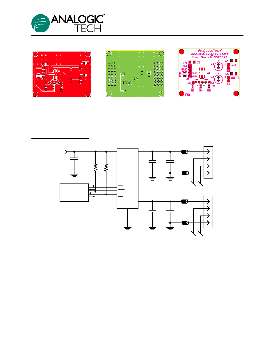
Figure 4: Evaluation board
Figure 5: Evaluation board
Figure 6: Evaluation board
component side layout
solder side layout
top side silk screen layout /
assembly drawing
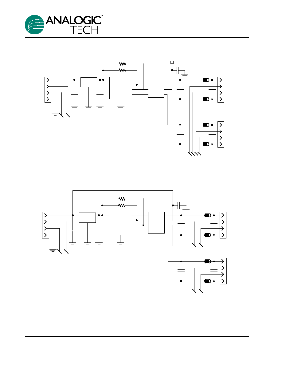
Application Circuits
Figure 7: Typical Dual USB Host Port Application
C
IN
0.1
µ
F
R1
100k
On/Off A
Error Flag A
USB Controller
AAT4626
V
BUS
= 5.0V
IN
OUTA
FLGA
ENA
OUTB
8
7
2
1
6
C
OUT1
0.1
µ
F
C
OUT2
120
µ
F
DATA
(Port A)
D+
D-
V
BUS(A)
GND
Ferrite Beads
5
C
OUT3
0.1
µ
F
C
OUT4
120
µ
F
DATA
(Port B)
D+
D-
V
BUS(B)
GND
Ferrite Beads
Error Flag B
On/Off B
FLGB
ENB
3
4
R2
100k
AAT4626
USB Dual-Channel Power Switch
4626.2002.1.0.93
11
AAT4626
USB Dual-Channel Power Switch
12
4626.2002.1.0.93
Figure 8: Self-Powered Dual Port USB Hub
Figure 9: USB Bus Powered Dual Port USB Hub
120
µ
F
0.1
µ
F
0.1
µ
F
100k
1
µ
F
1
µ
F
AAT3200-3.3
3.3V USB Controller
AAT4626
Ferrite Beads
Data
Data A
V
BUS
D+
D-
GND
V
BUS(A)
D+
D-
GND
USB Port A
4.50V to 5.25V
Upstream V
BUS
100mA Maximum
VIN
ON/OFF A
Over Current A
IN
OUT
GND
GND
ENA
OUTA
FLGA
FLGB
ENB
OUTB
GND
IN
100k
Over Current B
ON/OFF B
120
µ
F
0.1
µ
F
Ferrite Beads
Data B
V
BUS(B)
D+
D-
GND
USB Port B
120
µ
F
0.1
µ
F
0.1
µ
F
100k
1
µ
F
1
µ
F
AAT3200-3.3
3.3V USB Controller
AAT4626
Ferrite Beads
Data
Data A/B
(Two Pair to
USB Controller)
V
BUS
D+
D-
GND
V
BUS(A)
D+
D-
GND
USB Port A
4.50V to 5.25V
Upstream V
BUS
100mA Maximum
VIN
ON/OFF A
Over Current A
IN
OUT
GND
GND
ENA
OUTA
FLGA
FLGB
ENB
OUTB
GND
IN
100k
Over Current B
ON/OFF B
120
µ
F
0.1
µ
F
Ferrite Beads
V
BUS(B)
D+
D-
GND
USB Port B
V
CC
+5.0V

AAT4626
USB Dual-Channel Power Switch
4626.2002.1.0.93
13
Ordering Information
Package Information
SOP-8
1 2
E
b
e
H
D
A1
A
A2
7 (4x)
c
L
y
Q
Package
Enable
Marking
Part Number
Bulk
Tape and Reel
SOP8
EN (Active-high)AAT4626IAS-1-B1
AAT4626IAS-1-T1
SOP8
EN (Active-low)AAT4626IAS-B1
AAT4626IAS-T1
TSSOP8
EN (Active-high)AAT4626IHS-1-B1
AAT4626IHS-1-T1
TSSOP8
EN (Active-low)AAT4626IHS-B1
AAT4626IHS-T1
Dim
Millimeters
Inches
Min
Max
Min
Max
A
1.35
1.75
0.053
0.069
A1
0.10
0.25
0.004
0.010
A2
1.45
0.057
B
0.33
0.51
0.013
0.020
C
0.19
0.25
0.007
0.010
D
4.80
5.00
0.189
0.197
E
3.80
4.00
0.150
0.157
e
1.27
0.050
H
5.80
6.20
0.228
0.244
L
0.40
1.27
0.016
0.050
Y
0.00
0.10
0.000
0.004
1
0∞
8∞
0∞
8∞
Note:
1. PACKAGE BODY SIZES EXCLUDE MOLD FLASH
PROTRUSIONS OR GATE BURRS.
2. TOLERANCE 0.1000mm (4mil) UNLESS
OTHERWISE SPECIFIED
3. COPLANARITY: 0.1000mm
4. DIMENSION L IS MEASURED IN GAGE PLANE.
5. CONTROLLING DIMENSION IS MILLIMETER;
CONVERTED INCH DIMENSIONS ARE NOT
NECESSARILY EXACT.

TSSOP-8
A1
b
e
E
1 2
A
A2
E1
DETAIL A
R
L1
L
0.20
D
R1
2
E
1
DETAIL A
AAT4626
USB Dual-Channel Power Switch
14
4626.2002.1.0.93
Advanced Analogic Technologies, Inc.
1250 Oakmead Parkway, Suite 310, Sunnyvale, CA 94086
Phone (408) 524-9684
Fax (408) 524-9689
Dim
Millimeters
Inches
Min
Max
Min
Max
A
1.05
1.20
0.041
0.047
A1
0.05
0.15
0.002
0.006
A2
-
1.05
-
0.041
b
0.25
0.30
0.010
0.012
c
0.127
0.005
D-8
2.90
3.10
0.114
0.122
D-28
9.60
9.80
0.378
0.386
E
4.30
4.50
0.170
0.177
E1
6.20
6.60
0.244
0.260
e
0.65 BSC
0.025 BSC
L
0.50
0.70
0.20
0.028
L1
1.0
0.039
R
0.09
-
0.004
-
R1
0.09
-
0.004
-
1
0∞
8∞
0∞
8∞
2
12∞