
SmartSwitch
TM
AAT4651
5V/3V PC Card Power Switch
4651.2006.05.1.2
1
General Description
The AAT4651 SmartSwitch is a single channel PC
card (PCMCIA) power switch. It is used to select
between two different voltage inputs, each between
2.7V and 5.5V. An internal switch powers the cir-
cuitry from whichever input voltage is higher. The
device's output, V
CC
, is slew rate controlled and cur-
rent limited, in compliance with PC card specifica-
tions. The current limit response time to a short cir-
cuit is typically 1µs. The internal P-channel MOS-
FET switches are configured to break before make;
that is, both switches cannot be closed at the same
time. Controlled by a 2-bit parallel interface, the
three states for V
CC
are V
CC5
, V
CC3
, or ground.
When in the ground state, V
CC
is pulled to ground by
an 200
resistor. An open drain FAULT output is
asserted during over-current conditions. During
power-up slewing, FAULT also signals that V
CC
is
out of tolerance. An internal over-temperature sen-
sor forces V
CC
to a high impedance state when an
over-temperature condition exists. Quiescent cur-
rent is typically a low 15µA, as long as I
CC
is less
than approximately 500mA. Above this load current,
the quiescent current increases to 200µA.
The AAT4651 is available in a Pb-free, 8-pin SOP
or TSSOP package and is specified over the -40∞C
to +85∞C temperature range.
Features
∑
2.7V to 5.5V Input Voltage Range
∑
80m
(5V) Typical R
DS(ON)
∑
Low Quiescent Current: 15µA (Typ)
∑
Reverse-Blocking Switches
∑
Short-Circuit Protection
∑
Over-Temperature Protection
∑
FAULT Flag Output
∑
Temperature Range: -40∞C to +85∞C
∑
8-Pin SOP or TSSOP Package
Applications
∑
Notebook Computer
∑
PDA, Subnotebook
∑
Power Supply Multiplexer Circuit
Typical Application
C
OUT
0.1
F
VCC5
C
IN5
1
F
C
IN3
1
F
VCC3
VCCD1
VCCD0
FAULT
VCC
GND
AAT4651
8
5
2
3
4
1
6,7
VCC3
VCC5
GND
GND
VCC
VCCD1
VCCD0
FAULT

Pin Descriptions
Pin Configuration
SOP-8
TSSOP-8
(Top View)
(Top View)
Control Logic Table
VCCD1
VCCD0
Function
Result
0
0
OFF
80
V
CC
to GND
0
1
3.3V
V
CC
= V
CC3
1
0
5V
V
CC
= V
CC5
1
1
OFF
80
V
CC
to GND
GND
VCCD1
VCCD0
FAULT
VCC5
VCC
VCC
VCC3
4
3
2
1
5
6
7
8
1
2
VCC
VCC5
VCC
VCC3
GND
VCCD1
VCCD0
FAULT
1
2
3
4
8
7
6
5
Pin #
Symbol
Function
1
GND
Ground connection.
2
VCCD1
Control input (see Control Logic Table below).
3
VCCD0
Control input (see Control Logic Table below).
4
FAULT
Open drain output; signals over-current condition.
5
VCC3
3V supply.
6, 7
VCC
Output (see Control Logic Table below).
8
VCC5
5V supply.
AAT4651
5V/3V PC Card Power Switch
2
4651.2006.05.1.2
Absolute Maximum Ratings
1
T
A
= 25∞C, unless otherwise noted.
Thermal Characteristics
3
Symbol
Description
Value
Units
JA
Thermal Resistance
SOP-8
120
∞C/W
TSSOP-8
150
P
D
Power Dissipation
SOP-8
1.0
W
TSSOP-8
833
mW
Symbol
Description
Value
Units
V
CC3
, V
CC5
IN to GND
-0.3 to 6
V
V
CC
OUT to GND
-0.3 to 6
V
I
MAX
Maximum Continuous Switch Current
Current Limited
A
T
J
Operating Junction Temperature Range
-40 to 150
∞C
V
ESD
ESD Rating
2
-- HBM
4000
V
AAT4651
5V/3V PC Card Power Switch
4651.2006.05.1.2
3
1. Stresses above those listed in Absolute Maximum Ratings may cause permanent damage to the device. Functional operation at condi-
tions other than the operating conditions specified is not implied. Only one Absolute Maximum Rating should be applied at any one time.
2. Human body model is a 100pF capacitor discharged through a 1.5k
resistor into each pin.
3. Mounted on an FR4 board.

Electrical Characteristics
V
CC5
= 5.0V, V
CC3
= 3.3V, T
A
= -40∞C to +85∞C, unless otherwise noted. Typical values are at T
A
= 25∞C; bold
values designate full temperature range.
Symbol
Description
Conditions
Min Typ Max Units
V
CC
Output
Iccsc
Short-Circuit Current Limit
V
CC
= V
CCIN
-0.5V, On Mode V
CC3
1.0
2.5
A
or V
CC5
Selected, T
A
= 25∞C
V
CC
= 3.0V, T
A
= 25∞C
85
110
m
R
DS(ON)
On Resistance
V
CC
= 5.0V, T
A
= 25∞C
80
100
R
CLAMP
Clamp Resistance
V
CC
= Clamped to GND,
80
200
I
CCOUT
= 10mA Sinking
Tcrds
Switch Resistance
2800
ppm/∞C
Temperature Coefficient
V
CC
Switching Time (Refer to Figure 1)
t1
Output Turn-On Delay Time
V
CC
= 0V to 10% of 3.3V, R
OUT
= 10
500
2000
t2
Output Turn-On Delay Time
V
CC
= 0V to 10% of 5.0V, R
OUT
= 10
500
1500
t3
Output Rise Time
V
CC
= 10% to 90% of 3.3V, R
LOAD
= 10
300
1000 3000
t4
Output Rise Time
V
CC
= 10% to 90% of 5.0V, R
LOAD
= 10
300
1000 3000
µs
t5
Output Turn-Off Delay Time
V
CC
= 3.3V to 90% of 3.3V, R
LOAD
= 10
400
t6
Output Turn-Off Delay Time
V
CC
= 5.0V to 90% of 5.0V, R
LOAD
= 10
400
t7
Output Fall Time to Off State
V
CC
= 90% to 10% of 3.3V, R
LOAD
= 10
200
t8
Output Fall Time to Off State
V
CC
= 90% to 10% of 5.0V, R
LOAD
= 10
200
Power Supply
V
CC3
V
CC3
Operation Voltage
2.7
5.5
V
V
CC5
V
CC5
Operation Voltage
2.7
5.5
V
V
CC
= 5V or Off, V
CC3
< V
CC5
,
1
I
CC3
V
CC3
Supply Current
I
CC
Out = 0
µA
V
CC
= 3.3V, V
CC3
< V
CC5
, I
CC
Out = 0
5
20
I
CC5
V
CC5
Supply Current
V
CC
= Off, V
CC5
> V
CC3
, I
CC
Out = 0
1
V
CC
= 3.3V, V
CC5
> V
CC3
, I
CC
Out = 0
10
40
µA
V
CC
= 5V, V
CC5
> V
CC3
, I
CC
Out = 0
15
40
Parallel Interface
VCCD LOW VCCD Input Low Voltage
V
CC3
or V
CC5
= 3.0V to 5.5V
1
0.8
V
VCCD HI
VCCD Input High Voltage
V
CC3
or V
CC5
= 2.7V to 3.6V
2.0
V
V
CC3
or V
CC5
= 4.5V to 5.5V
2.4
I
SINK VCCD
VCCD Input leakage
V
CTL
= 5.5V
0.01
1
µA
V
FAULTLOW
FAULT Logic Output Low
I
SINK
= 1mA
0.4
V
Voltage
I
SINKFAULT
FAULT Logic Output High
V
FAULT
= 5.5V
0.05
1
µA
Leakage Current
Other
OTMP
Over-Temperature Shutdown
125
∞C
AAT4651
5V/3V PC Card Power Switch
4
4651.2006.05.1.2
1. For VCCD outside this range, consult Typical VCCD Threshold curve.

Typical Characteristics
Unless otherwise noted, T
A
= 25∞C.
R
DS(ON)
vs. Temperature
60.0
70.0
80.0
90.0
100.0
110.0
120.0
-40
-20
0
20
40
60
80
100
120
Temperature (
∞C)
R
DS(ON)
(m
)
V
CC
= V
CC3
= 3.0V
V
CC
= V
CC5
= 5.0V
Off-Switch Current vs. Temperature
(I
CC5
)
0.0000
0.0001
0.0010
0.0100
0.1000
1.0000
-40
-20
0
20
40
60
80
100
120
Temperature (
∞C)
V
CC5
= 5V
V
CC3
= 3V
VCCD1 = 0V
VCCD0 = 0V
Off-Switch Current (
A)
Off-Switch Current vs. Temperature
(I
CC3
)
0.0000
0.0001
0.0010
0.0100
0.1000
1.0000
-40
-20
0
20
40
60
80
100
120
Temperature (
∞C)
V
CC3
= 3V
V
CC5
= 5V
VCCD1 = 0V
VCCD0 = 0V
Off-Switch Current (
A)
Current Limit
(V
CC
= V
CC5
)
0
0.5
1
1.5
2
0
1
2
3
4
5
6
Output Voltage (V)
Current Limit
(V
CC
= V
CC3
)
0
0.5
1
1.5
2
0
0.5
1
1.5
2
2.5
3
Output Voltage (V)
Quiescent Current vs. Temperature
(I
CC5
)
0
5
10
15
20
25
30
-40
-20
0
20
40
60
80
100
120
Temperature (
∞C)
V
CC3
= 3V
V
CC5
= 5V
VCCD1
VCCD0 = 0V
= 5V
Quiescent Current (
A)
AAT4651
5V/3V PC Card Power Switch
4651.2006.05.1.2
5

AAT4651
5V/3V PC Card Power Switch
6
4651.2006.05.1.2
Typical Characteristics
Unless otherwise noted, T
A
= 25∞C.
VCCD Threshold vs. V
CC
0.5
0.7
0.9
1.1
1.3
1.5
1.7
1.9
2.1
2.3
2.5
2.5
3.0
3.5
4.0
4.5
5.0
5.5
V
CC
(V)
VCCD Threshold Voltage (V)
VCCDH
VCCDL
Short Circuit Through 0.6
0
2
4
6
8
-2
0
2
4
6
8
10
Input and Output (V)
Output (A)
-3
0
3
6
9
Input Voltage
Time (
s)
Output Voltage
Output Current
Short Circuit Through 0.3
0
2
4
6
8
-2
0
2
4
6
8
10
Time
Output (A)
Input and Output (V)
(
s)
-1
2
5
8
11
Input Voltage
Output Current
Output Voltage
Thermal Shutdown Response
(VCCD0 = 0V)
Time (100ms/div)
VCCD1 (5V/div)
FAULT (5V/div)
V
CC
(1V/div)
I
VCC5
(500mA/div)
VCCD1 (5V/div)
V
CC
(1V/div)
I
VCC5
(200mA/div)
FAULT (5V/div)
Time (500µs/div)
Turn-On/Off Response with 15
, 1F Load
(VCCD0 = 0V)
Turn-On/Off Response with 10, 1µF Load
(VCCD1 = 0V)
VCCD0 (5V/div)
V
CC
(2V/div)
FAULT (5V/div)
Time (500µs/div)
I
VCC5
(500mA/div)

AAT4651
5V/3V PC Card Power Switch
4651.2006.05.1.2
7
Functional Description
The AAT4651 is a single channel power switch that
can be used in any application where dual power
supply multiplexing is required. Typical applications
for this include PC card applications not requiring a
12V power supply, or applications where power is
switched, for example, between 5V for operation
and 3.3V for standby mode. The AAT4651 operates
with input voltages ranging from 2.7V to 5.5V in any
combination and automatically powers its internal
circuitry from whichever input voltage is higher. Two
identical low R
DS(ON)
P-channel MOSFETs serve as
the power multiplexing circuit with a common drain
as the V
CC
output and independent sources as the
two V
CC3
and V
CC5
inputs. A 2-bit parallel interface
determines the state of the multiplexer: V
CC
= V
CC3
,
V
CC
= V
CC5
, or V
CC
with resistive pull down to
ground. When the state is set to either of the two
inputs, the multiplexing circuit will slowly slew the
V
CC
output to the new voltage level which protects
the upstream power supply from sudden load tran-
sients. When the resistive pull down is chosen for
V
CC
, the V
CC
output is quickly discharged by the
resistive pull down. The AAT4651 always serves as
an electronic fuse by limiting the load current if it
exceeds the current limit threshold. During power-
up into a short, the current will gradually increase
until the current limit is reached. During a sudden
short circuit on the output, the current limit will
respond in 1µs to isolate and protect the upstream
power supply from the load short circuit. In most
applications, because the response time is so fast,
a short circuit to V
CC
will not affect the upstream
supply, so system functionality will not be affected.
In the case of an over-current condition, an open
drain FAULT flag output will signal the event. The
FAULT output is also active during output voltage
slew, and becomes inactive once the output is with-
in regulation.
Functional Block Diagram
Body Control
80
V
CC3
V
CC5
V
CC
VCCD0
VCCD1
FAULT
GND
Over-
Temperature
Over-
Current
Over-
Current
Control
Logic
Slew
Rate
Slew
Rate

Applications Information
Input Capacitor
A 1µF or larger capacitor is typically recommended
for C
IN
. A C
IN
capacitor is not required for basic
operation; however, it is useful in preventing load
transients from affecting upstream circuits. C
IN
should be located as close to the device VIN pin as
practically possible. Ceramic, tantalum, or alu-
minum electrolytic capacitors may be selected for
C
IN
. There is no specific capacitor equivalent series
resistance (ESR) requirement for C
IN
. However, for
higher current operation, ceramic capacitors are rec-
ommended for C
IN
due to their inherent capability
over tantalum capacitors to withstand input current
surges from low impedance sources such as batter-
ies in portable devices.
Output Capacitor
A 0.1µF or greater capacitor is generally required
between V
CC
and GND. Likewise, with the output
capacitor, there is no specific capacitor ESR
requirement. If desired, C
OUT
may be increased to
accommodate any load transient condition.
Parallel Interface / Break Before Make
A 2-bit parallel interface determines the state of the
V
CC
output. The logic levels are compatible with
CMOS or TTL logic. A logic low value must be less
than 0.8V, and a logic high value must be greater
than 2.4V. In cases where the interface pins rapidly
change state directly from 3V to 5V (or vice versa),
internal break-before-make circuitry prevents any
backflow of current from one input power supply to
the other. In addition, the body connections of the
internal P-channel MOSFET switches are always
set to the highest potential of V
CC3
, V
CC5
, or V
CC
,
which prevents any body diode conduction, power
supply backflow, or possible device damage.
FAULT Output
The FAULT output is pulled to ground by an open
drain N-channel MOSFET during an over-current
or output slew condition. It should be pulled up to
the reference power supply of the controller IC via
a nominal 100k
resistor.
Voltage Regulation
The PC card specification calls for a regulated 5V
supply tolerance of +/-5%. Of this, a typical power
supply will drop less than 2%, and the PCB traces
will drop another 1%. This leaves 2% for the
AAT4651 as the PC card switch. In the PC card
application, the maximum allowable current for the
AAT4651 is dominated by voltage regulation rather
than by thermal considerations, and is set by either
the current limit or the maximum R
DS(ON)
of the P-
channel MOSFET. The maximum R
DS(ON)
at 85∞C
is calculated by applying the R
DS(ON)
temperature
coefficient to the maximum room temperature
R
DS(ON)
:
-or-
The maximum current is equal to the 2% tolerance
of the 5V supply (100mV) across the AAT4651
divided by R
DS(ON)(MAX)
. Or:
For the 3.3V supply in the PC card application, the
conditions are a bit relaxed, with the allowable volt-
age regulation drop equal to 300mV. With a 2%
supply and 1% PCB trace regulation, the PC card
switch can have a 200mV drop. So:
Since 1.5A is the nominal current limit value, the
AAT4651 will current limit before I
MAX3
is reached.
Thermal issues are not a problem in the SOP-8
package since
JA
, the package thermal resistance,
is only 120∞C/W. At any given ambient temperature
I
MAX3
=
= 1.5A
200mV
134m
I
MAX5
=
= 856.2mA
100mV
116.8m
R
DS(ON)(MAX)
= 100m
(1 + [0.0028 60]) = 116.8m
R
DS(ON)(MAX)
= R
DS(ON)25
(1 + [TC T])
AAT4651
5V/3V PC Card Power Switch
8
4651.2006.05.1.2

AAT4651
5V/3V PC Card Power Switch
4651.2006.05.1.2
9
(T
A
), the maximum package power dissipation can
be determined by the following equation:
Constants for the AAT4651 are maximum junction
temperature, T
J(MAX)
= 125∞C, and package thermal
resistance,
JA
= 120∞C/W. Worst case conditions
are calculated at the maximum operating tempera-
ture where T
A
= 85∞C. Typical conditions are cal-
culated under normal ambient conditions where T
A
= 25∞C. At T
A
= 85∞C, P
D(MAX)
= 333mW. At T
A
=
25∞C, P
D(MAX)
= 833mW.
Maximum current is given by the following equation:
For the AAT4651 at 85∞C, I
OUT(MAX)
= 1.65A, a
value greater than the internal minimum current
limit specification.
Over-Current and Over-Temperature
Protection
Because many AAT4651 applications provide power
to external devices, it is designed to protect its host
device from malfunctions in those peripherals
through slew rate control, current limiting, and ther-
mal limiting. The AAT4651 current limit and thermal
limit serve as an immediate and reliable electronic
fuse without any increase in R
DS(ON)
for this function.
Other solutions, such as a poly fuse, do not protect
the host power supply and system from mishandling
or short circuiting peripherals; they will only prevent
a fire. The AAT4651 high-speed current limit and
thermal limit not only prevent fires, they also isolate
the power supply and entire system from any activi-
ty at the external port and report a mishap by means
of a FAULT signal.
Over-current and over-temperature go hand in hand.
Once an over-current condition exists, the current
supplied to the load by the AAT4651 is limited to the
over-current threshold. This results in a voltage drop
across the AAT4651 which causes excess power
dissipation and a package temperature increase. As
the die begins to heat up, the over-temperature cir-
cuit is activated. If the temperature reaches the
maximum level, the AAT4651 automatically switches
off the P-channel MOSFETs. While they are off, the
over-temperature circuit remains active. Once the
temperature has cooled by approximately 10∞C, the
P-channel MOSFETs are switched back on. In this
manner, the AAT4651 is thermally cycled on and off
until the short circuit is removed. Once the short is
removed, normal operation automatically resumes.
To save power, the full high-speed over-current cir-
cuit is not activated until a lower threshold of cur-
rent (approximately 500mA) is exceeded in the
power device. When the load current exceeds this
crude threshold, the AAT4651 quiescent current
increases from 15µA to 200µA. The high-speed
over-current circuit works by linearly limiting the
current when the current limit is reached. As the
voltage begins to drop on V
CC
due to current limit-
ing, the current limit magnitude varies and general-
ly decreases as the V
CC
voltage drops to 0V.
Switching V
CC
Voltage
The AAT4651 meets PC card standards for switch-
ing the V
CC
output by providing a ground path for
V
CC
as well as "off" state. The PC card protocol for
determining low voltage operations is to first power
the peripheral with 5V and poll for 3.3V operation.
When transitioning from 5V to 3.3V, V
CC
must be
discharged to less than 0.8V to provide a hard
reset. The resistive ground state (VCCD0 =
VCCD1) will accommodate this. The ground state
will also guarantee the V
CC
voltage to be discharged
within the specified 100ms amount of time.
Printed Circuit Board Layout
Recommendations
For proper thermal management, to minimize PCB
trace resistance, and to take advantage of the low
R
DS(ON)
of the AAT4651, a few circuit board layout
rules should be followed: V
CC3
, V
CC5
, and V
CC
should be routed using wider than normal traces;
the two V
CC
pins (Pins 6 and 7) should be con-
nected to the same wide PCB trace; and GND
should be connected to a ground plane. For best
performance, C
IN
and C
OUT
should be placed close
to the package pins.
=
I
OUT(MAX)
P
D(MAX)
R
DS(ON)
P
D(MAX)
=
T
J(MAX)
-T
A
JA

AAT4651
5V/3V PC Card Power Switch
10
4651.2006.05.1.2
Timing Diagram
Figure 1: VCC Switching Time Diagram.
Refer to V
CC
Switching Time specifications in the Electrical Characteristics section of this datasheet for definitions of t1 to t8.
Typical PC Card Application Circuit
VCC5
VCC3
VCCD1
VCCD0
FAULT
VCC
GND
AAT4651
8
5
2
3
4
1
6,7
V
CC
Power
Supply
5V
3.3V
PC Card
Controller
PC Card
Slot
VCC_EN1
VCC_EN0
FAULT
100k
V
CC
C
IN3
1
F
C
IN5
1
F
C
OUT
0.1
F
0
5
VCCD0,1
Vcc
t3, t4
t1, t2
t5, t6
t7, t8
0
5
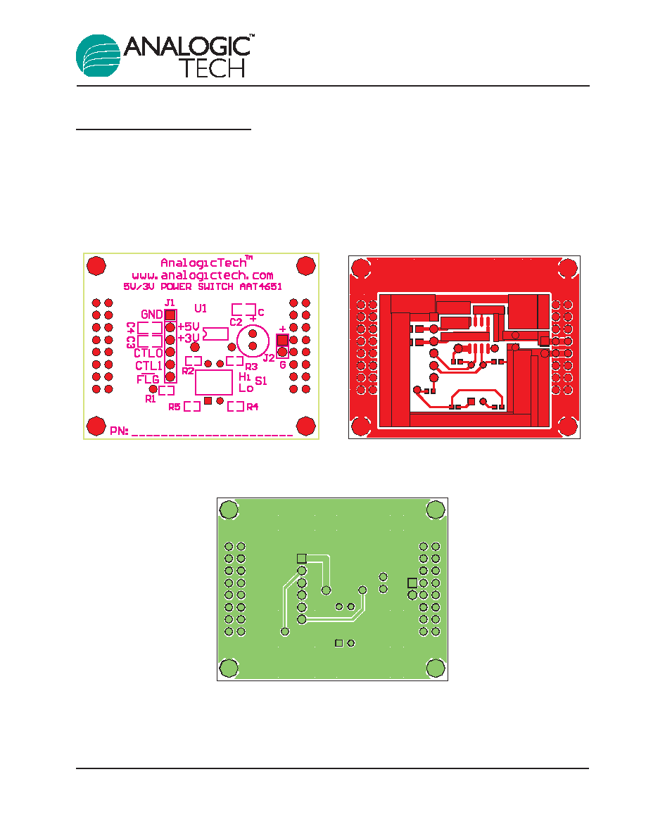
Evaluation Board Layout
The AAT4651 evaluation board layout follows the
printed circuit board layout recommendations, and
can be used for good applications layout.
Note: Board layout shown is not to scale.
AAT4651
5V/3V PC Card Power Switch
4651.2006.05.1.2
11
Figure 2: Evaluation Board Top Side
Figure 3: Evaluation Board
Silk Screen Layout / Assembly Drawing.
Component Side Layout.
Figure 4: Evaluation Board
Solder Side Layout.

AAT4651
5V/3V PC Card Power Switch
12
4651.2006.05.1.2
Ordering Information
Package Information
SOP-8
All dimensions in millimeters.
0.175
±
0.075
6.00
±
0.20
3.90
±
0.10
1.55
±
0.20
1.27 BSC
0.42
± 0.09 ◊ 8
4.90
± 0.10
4
∞
±
4
∞
45
∞
0.375
± 0.125
0.235
± 0.045
0.825
± 0.445
All AnalogicTech products are offered in Pb-free packaging. The term "Pb-free" means
semiconductor products that are in compliance with current RoHS standards, including
the requirement that lead not exceed 0.1% by weight in homogeneous materials. For more
information, please visit our website at http://www.analogictech.com/pbfree.
Package
Marking
Part Number (Tape and Reel)
1
SOP-8
4651
AAT4651IAS-T1
TSSOP-8
4651
AAT4651IHS-T1
1. Sample stock is generally held on part numbers listed in BOLD.
AAT4651
5V/3V PC Card Power Switch
4651.2006.05.1.2
13
TSSOP-8
All dimensions in millimeters.
DETAIL A
4.40
±
0.10
6.40
±
0.20
0.65 BSC
3.00
± 0.10
0.245
± 0.055 ◊ 8
0.10
± 0.05
0.60
± 0.15
0.145
± 0.055
1.05 MAX
1.20 MAX
4
∞ ± 4∞
12
∞
12
∞ REF ◊ 4
1.00
REF

AAT4651
5V/3V PC Card Power Switch
14
4651.2006.05.1.2
Advanced Analogic Technologies, Inc.
830 E. Arques Avenue, Sunnyvale, CA 94085
Phone (408) 737-4600
Fax (408) 737-4611
© Advanced Analogic Technologies, Inc.
AnalogicTech cannot assume responsibility for use of any circuitry other than circuitry entirely embodied in an AnalogicTech product. No circuit patent licenses, copyrights, mask work rights,
or other intellectual property rights are implied. AnalogicTech reserves the right to make changes to their products or specifications or to discontinue any product or service without notice.
Customers are advised to obtain the latest version of relevant information to verify, before placing orders, that information being relied on is current and complete. All products are sold sub-
ject to the terms and conditions of sale supplied at the time of order acknowledgement, including those pertaining to warranty, patent infringement, and limitation of liability. AnalogicTech
warrants performance of its semiconductor products to the specifications applicable at the time of sale in accordance with AnalogicTech's standard warranty. Testing and other quality con-
trol techniques are utilized to the extent AnalogicTech deems necessary to support this warranty. Specific testing of all parameters of each device is not necessarily performed.
AnalogicTech and the AnalogicTech logo are trademarks of Advanced Analogic Technologies Incorporated. All other brand and product names appearing in this document are regis-
tered trademarks or trademarks of their respective holders.