 | –≠–ª–µ–∫—Ç—Ä–æ–Ω–Ω—ã–π –∫–æ–º–ø–æ–Ω–µ–Ω—Ç: AAT4682 | –°–∫–∞—á–∞—Ç—å:  PDF PDF  ZIP ZIP |
SmartSwitch
TM
General Description
The AAT4682 Dual Electronic Resettable fuse is
part of the AnalogicTech Application Specific Power
MOSFET (ASPMTM) line of products. It has two 1A
current limited P-channel MOSFET power devices
that remain fully enhanced as long as the input
power supply is above an under voltage lockout
threshold, and the load is below the current limit
setting. If the load increases above the current limit
setting, as is the case during a short circuit, the
MOSFET effectively becomes a constant current
source equal to the current limit. If the current limit
condition persists long enough to heat the MOSFET
to an extreme temperature, both devices will ther-
mal cycle off and on until the current limit condition
is removed. Independent open drain FAULT flags
signal an over current or over temperature condi-
tion. Quiescent current typically is a low 10µA.
The AAT4682 is available in a 6 pin SOT-23, spec-
ified over a -40 to 85∞C temperature range.
Features
∑
Dual P-Channel MOSFETS
∑
500mA steady state load current
∑
600mA minimum current limit trip point
∑
Low quiescent current, typically 10µA.
∑
Over temperature protection
∑
Fast transient response:
∑
< 1µs response to short circuit
∑
400m
typical R
DS(ON)
∑
Undervoltage Lockout
∑
Temp range -40 to 85∞C
∑
FAULT flag with 2ms blanking
∑
6-pin SOT23 package
Applications
∑
USB ports
∑
Peripheral ports
∑
Desktop PCs
∑
Cell phone ports
AAT4682
Dual Electronic Resettable Switches
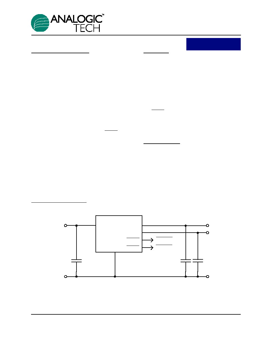
Typical Application
C
OUTA
1
µ
F
IN
C
IN
1
µ
F
FAULTA
OUTA
GND
AAT4682
5
2
6
INPUT
GND
GND
OUTA
FAULTA
FAULTB
FAULTB
OUTB
4
OUTB
C
OUTB
1
µ
F
3
1
Preliminary
Information
4682.2001.11.0.9
1

Pin Descriptions
Pin Configuration
SOT23-6
1
2
3
IN
OUTA
OUTB
4
6
5
FAULTA
FAULTB
GND
Pin #
Symbol
Function
1
FAULTA
Channel A open drain output signals over-current and over-temperature condition
2
GND
Ground connection
3
FAULTB
Channel B open drain output signals over-current and over-temperature condition
4
OUTB
Channel B P-channel MOSFET drain
5
IN
Channel A and Channel B P-channel MOSFET sources
6
OUTA
Channel A P-channel MOSFET drain
AAT4682
Dual Electronic Resettable Switches
2
4682.2001.11.0.9
Absolute Maximum Ratings
(T
A
=25∞C unless otherwise noted)
Note: Stresses above those listed in Absolute Maximum Ratings may cause permanent damage to the device. Functional operation at con-
ditions other than the operating conditions specified is not implied. Only one Absolute Maximum rating should be applied at any one time.
Note 1: Human body model is a 100pF capacitor discharged through a 1.5k
resistor into each pin.
Thermal Characteristics
Note 2: Mounted on a demo board.
Electrical Characteristics
(V
IN
= 5V, T
A
= -40 to 85∞C unless otherwise noted. Typical values
are at T
A
=25∞C; bold values designate full temperature range)
Symbol
Description
Conditions
Min
Typ
Max
Units
V
IN
Operation Voltage
1.8
5.5
V
I
Q
Quiescent Current
V
IN
= 5V, I
OUT
= 0
10
20
µA
V
UVLO
Undervoltage Lockout
V
IN
falling
1.5
V
V
UVLO(hys)
Undervoltage Lockout Hysteresis
0.3
V
R
DS(ON)
On-Resistance
V
IN
= 5.0V,T
A
= 25∞C
400
500
m
V
IN
= 3.V,T
A
= 25∞C
525
650
I
LIM
Current Limit
OUT < IN - 0.5V
0.6
0.875
1.25
A
t
RESP
Current Loop Response
V
IN
= 5V
500
ns
V
FAULTLOW
FAULT Logic Output Low
I
SINK
= 1mA
0.4
V
I
SINK
FAULT Logic Output High
V
FAULT
= 5.5V
0.5
1
µA
Leakage Current
T
blank
FAULT Blanking Time
2
ms
T
SD
Over-temperature threshold
125
∞C
Symbol
Description
Value
Units
JA
Maximum Thermal Resistance
2
150
∞C/W
P
D
Maximum Power Dissipation
2
667
mW
Symbol
Description
Value
Units
V
IN
IN to GND
-0.3 to 6
V
V
OUT
OUTA or OUTB to GND
-0.3 to 6
V
V
FLG
FAULTA or FAULTB to GND
-0.3 to 6
V
I
OUT
Output Current
Internally Limited
A
T
J
Operating Junction Temperature Range
-40 to 150
∞C
V
ESD
ESD Rating
1
- HBM
5000
V
T
LEAD
Maximum Soldering Temperature (at Leads)
300
∞C
AAT4682
Dual Electronic Resettable Switches
4682.2001.11.0.9
3
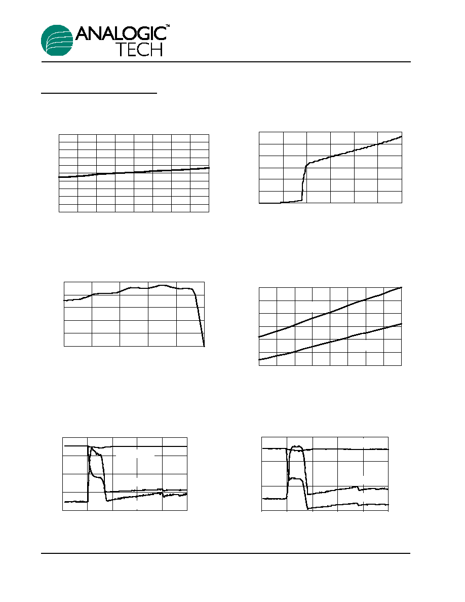
Typical Characteristics
(Unless otherwise noted, V
IN
= 5V, T
A
= 25∞C)
Short Circuit Through 0.6
0
2
4
6
-0.5
0.0
0.5
1.0
1.5
2.0
Time (
µ
s)
Input and Output (V)
-1
1
3
5
Output (A)
Input Voltage
Output Voltage
Output Current
Short Circuit Through 0.3
-2
0
2
4
6
-0.5
0.0
0.5
1.0
1.5
2.0
Time (
µ
s)
Input and Output (V)
-1
1
3
5
7
Output (A)
Input Voltage
Output Voltage
Output Current
R
DS
(ON) vs. Temperature
300
350
400
450
500
550
600
-40
-20
0
20
40
60
80
100
120
Temperature (
∞
C)
R
DS
(ON) (m
)
V
IN
=3V
V
IN
=5V
Current Limit vs. Output Voltage
0.0
0.2
0.4
0.6
0.8
1.0
0
1
2
3
4
5
Output (V)
Output (A)
Quiescent Current vs. Input Voltage
0
2
4
6
8
10
12
0
1
2
3
4
5
6
Input (V)
Quiescent Current (
µ
A)
Quiescent Current vs. Temperature
0
2
4
6
8
10
12
14
16
18
20
-40
-20
0
20
40
60
80
100
120
Temperature (
∞
C)
Quiescent Current (
µ
A)
AAT4682
Dual Electronic Resettable Switches
4
4682.2001.11.0.9

Typical Characteristics
(Unless otherwise noted, V
IN
= 5V, T
A
= 25∞C)
Fault Delay
500
µ
s/div
FAULTA (5V/div)
OUTA (5V/div)
FAULTB (5V/div)
OUTB (5V/div)
I
IN
(1A/div)
Thermal Shutdown Response
50ms/div
FAULTA (5V/div)
I
IN
(1A/div)
OUTA (5V/div)
FAULTB
(5V/div)
OUTB
(5V/div)
AAT4682
Dual Electronic Resettable Switches
4682.2001.11.0.9
5
Functional Description
The AAT4682 is a dual channel electronic reset-
table fuse that protects against short circuit condi-
tions by current limiting to a preset level. A patent-
ed fast acting current limit loop limits load current in
a fraction of a microsecond, and instantly resets
back to a low impedance state once the short cir-
cuit condition is removed. A current limit condition
is reported by the open drain FAULT output after a
two millisecond blanking interval. The blanking
prevents false reporting during the charging of a
capacitive load, which typically occurs when a load
is connected. The AAT4682 is internally protected
from thermal damage by an over temperature
detection circuit. If the die temperature reaches the
internal thermal limit, both power devices are
switched off until the die temperature cools to a
level below the thermal limit threshold. The device
will thermal cycle indefinitely until the over current
condition is removed. Due to the high thermal con-
ductivity of silicon and the size of the die, the tem-
perature across the die is relatively uniform at high
temperatures, and therefore, as a precaution, both
power devices are switched off when the thermal
threshold is reached. The AAT4682 operates with
input voltages ranging from 1.8V to 5.5V which,
along with its extremely low operating current,
makes it ideal for battery-powered applications. In
cases where the input voltage drops below 1.8V,
the AAT4682 internal MOSFETS are protected
from entering the saturated region of operation by
being automatically shut down by an undervoltage
lockout circuit.
The AAT4682 is ideally suited for protection of
peripheral ports such as USB, RS232 and parallel
ports.
AAT4682
Dual Electronic Resettable Switches
6
4682.2001.11.0.9
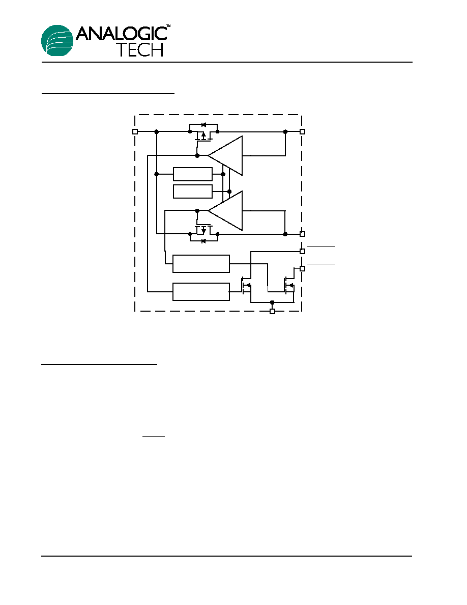
Functional Block Diagram
INA
OUTB
FAULTB
I
LIM
OTMP
UVLO
I
LIM
OUTB
FAULTA
GND
3ms Blanking
3ms Blanking

Applications Information
Input Capacitor
The input capacitor protects the power supply from
current transients generated by the loads attached to
the AAT4682. If a short circuit is suddenly applied to
a AAT4682 output, there is a 500 nanosecond long
period during which a large current can flow before
current limit circuitry activates. (See characteristic
curve "Short Circuit Through 0.3
.") In this event, a
properly sized input capacitor can dramatically
reduce the voltage transient seen by the power sup-
ply and other circuitry upstream from the AAT4682.
C
IN
should be located as close to the device V
IN
pin
as practically possible. Ceramic, tantalum or alu-
minum electrolytic capacitors may be selected for
C
IN
. There is no specific capacitor ESR requirement
for C
IN
. However, for higher current operation,
ceramic capacitors are recommended for C
IN
due to
their inherent capability over tantalum capacitors to
withstand input current surges from low impedance
sources such as batteries in portable devices.
Output Capacitors
In order to insure stability while current limit is
active, a small output capacitance of approximately
1µF is required at each output. No matter how big
the output capacitor, output current is limited to the
value set by the AAT4682 current limiting circuitry,
allowing very large output capacitors to be used.
For example, USB ports are specified to have at
least 120µF of capacitance down stream from their
controlling power switch. The current limiting circuit
will allow an output capacitance of 1000µF or more
without disturbing the upstream power supply.
Attaching Loads
Capacitive loads attached to the AAT4682 will charge
at a rate no greater than the current limit setting.
FAULT Outputs
FAULT flags are provided to alert a system if a
AAT4682 load is not receiving sufficient voltage to
operate properly. If current limit or over temperature
circuits in any combination are active for more than
approximately two milliseconds, the corresponding
FAULT output is pulled to ground through approxi-
mately 100
. Removal of voltage or current tran-
sients of less than two milliseconds prevents capaci-
tive loads connected to the AAT4682 output from acti-
vating the FAULT flag when they are initially attached.
Pull up resistances of 10k
to
100k
are recom-
mended. Since the FAULT outputs are open drain
terminals, they may be pulled up to any voltage rail
less than the maximum operating voltage of 5.5V,
allowing for level shifting between circuits.
Thermal Considerations
Since the AAT4682 has internal current limit and over
temperature protection, junction temperature is rarely
a concern. However, if the application requires large
currents in a hot environment, it is possible that tem-
perature rather than current limit will be the dominant
regulating condition. In these applications, the max-
imum combined current available without risk of an
over temperature condition can be calculated. The
maximum internal temperature while current limit is
not active can be calculated using Equation 1.
T
J(MAX)
= I
MAX
2
◊
R
DS(ON)
(MAX)
◊
R
JA
+ T
A
(MAX)
In Equation 1, I
MAX
is the maximum current
required by the load. R
DS(ON)
(MAX) is the maxi-
mum rated R
DS(ON)
of the AAT4682 at high temper-
ature. R
JA
is the thermal resistance between the
AAT4682 die and the board onto which it is mount-
ed. T
A
(MAX) is the maximum temperature that the
PCB under the AAT4682 would be if the AAT4682
were not dissipating power. Equation 1 can be
rearranged to solve for I
MAX
; Equation 2.
I
MAX
=
T
SD
(MIN) - T
A
(MAX)
R
DS(ON)
(MAX)
◊
R
JA
T
SD
(MIN) is the minimum temperature required to
activate the AAT4682 over temperature protection.
The typical over temperature threshold specifica-
tion is 125∞C, therefore 115∞C is a safe minimum
value to use.
For example, if an application is specified to oper-
ate in 50∞C environments, the PCB operates at
temperatures as high as 85∞C. The application is
sealed and its PCB is small, causing R
JA
to be
approximately 150∞C/W. Using Equation 2,
I
MAX
=
115 - 85
= 575mA
600
◊
150
To prevent thermal limiting, the combined operating
load current of each output in the application must
be less than 575mA.
AAT4682
Dual Electronic Resettable Switches
4682.2001.11.0.9
7
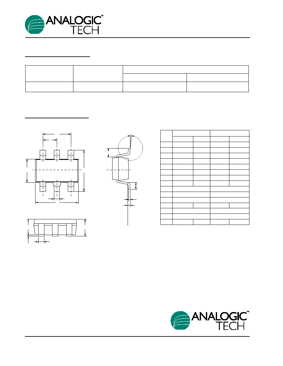
Ordering Information
Package Information
A1
b
A2
A
E
D
f
L2
t
L
C
GAUGE PLANE
e1
e
Package
Marking
Part Number
Bulk
Tape and Reel
SOT23-6
N/A
AAT4682IGU-T1
AAT4682
Dual Electronic Resettable Switches
8
4682.2001.11.0.9
Advanced Analogic Technologies, Inc.
1250 Oakmead Parkway, Suite 310, Sunnyvale, CA 94086
Phone (408) 524-9684
Fax (408) 524-9689
Dim
Millimeters
Inches
Min
Max
Min
Max
A
0.95
1.45
0.037
0.057
A1
0.05
0.15
0.002
0.006
A2
0.90
1.30
0.035
0.051
b
0.35
0.50
0.0137
0.019
c
0.08
0.20
0.0031
0.0078
D
2.84
3.00
0.1118
0.118
E
1.50
1.70
0.059
0.0669
E1
2.60
3.00
0.102
0.118
e
0.95 BSC
0.0374 BSC
e1
1.90 BSC
0.0748 BSC
f
0.50 BSC
0.0197 BSC
L
0.23
0.40
0.009
0.016
L1
0.10 BSC
0.039 BSC
L2
0.60 BSC
0.0236 BSC
t
0∫
10∫
0∫
10∫