 | –≠–ª–µ–∫—Ç—Ä–æ–Ω–Ω—ã–π –∫–æ–º–ø–æ–Ω–µ–Ω—Ç: AAT4900 | –°–∫–∞—á–∞—Ç—å:  PDF PDF  ZIP ZIP |

AAT4900
Buffered Power Half-Bridge
Advanced Analogic Technologies, Inc.
1250 Oakmead Pkwy, Suite 310, Sunnyvale, CA 94086
(408)524-9684 Fax (408)524-9689
4900.2000.9.0.71
General Description
The AAT4900 FastSwitch
‰ is a member of
AnalogicTech's Application Specific Power
MOSFET
‰ (ASPM‰) product family. It is a
Buffered Power Half-Bridge, consisting of low on-
resistance Power MOSFETs with integrated
control logic. This device operates with inputs
ranging from 2.7V to 5.5V, making it ideal for both
3V and 5V systems. The device is protected from
shoot-through current with its own control
circuitry. The AAT4900 is capable of very fast
switching times and is ideal for use in high
frequency DC to DC Converters. The quiescent
supply current is a low 1mA (max) at 1MHz CLK
frequency. In shutdown mode, the supply current
decreases to 1
µA max
The AAT4900 is available in 5 pin SOT-23
specified over -40 to 85
∞C.
Features
∑= 2.7V to 5.5V Input voltage range
∑= 120m (typ) Switch R
DS(ON)
∑= Low quiescent current
∑= 1µA (max) DC
∑= 1mA (max) at 1MHz
∑= Only 2.5V needed for Control Signal Input
∑= Temp range -40 to 85∞C
∑= 5 pin SOT-23 package
Applications
∑= High frequency DC/DC converters
∑= Low-side MOSFET gate driver
Typical Applications
Ad
van
ced
In
fo
rmatio
n
AAT4900
EN
IN
OUT
CLK
GND
ENABLE
2.7V to 5.5V Input
OUTPUT
5
3
1
2
4
Control Circuit
(PWM Output)
SOT-23
DC/DC Converter Output Stage
8-1
FastSwitch
TM

AAT4900
Buffered Power Half-Bridge
Advanced Analogic Technologies, Inc.
1250 Oakmead Pkwy, Suite 310, Sunnyvale, CA 94086
(408)524-9684 Fax (408)524-9689
4900.2000.9.0.71
Absolute Maximum Ratings
(T
A
=25
∞C unless otherwise noted)
Symbol
Description
Value
Units
V
IN
IN to GND
-0.3 to 6
V
V
EN
, V
CLK
EN, CLK to GND
-0.3 to
V
IN
+0.3
V
V
OUT
OUT to GND
-0.3 to
V
IN
+0.3
V
I
MAX
Maximum Continuous Switch Current
TBD
A
T
J
Operating Junction Temperature Range
-40 to 150
∞C
JA
Maximum Thermal Resistance
260
∞C/W
P
D
Maximum Power Dissipation
380
mW
T
LEAD
Maximum Soldering Temperature (at Leads)
300
∞C
Note: Stresses above those listed in Absolute Maximum Ratings may cause permanent damage to the device. Functional operation at
conditions other than the operating conditions specified is not implied. Only one Absolute Maximum rating should be applied at any one
time.
Electrical Characteristics
(V
IN
= 5V, T
A
= -40 to 85
∞C unless otherwise noted. Typical values are
at T
A
=25
∞C)
Symbol
Description
Conditions
Min
Typ
Max
Units
V
IN
Operation Voltage
2.7
5.5
V
I
QAC
AC Quiescent Current
IN = 5V, EN = IN,
CLK = 1MHz, I
OUT
= 0
1
mA
I
QDC
DC Quiescent Current
IN = 5V, EN = IN,
CLK = GND, I
OUT
= 0
1
µA
I
Q(OFF)
Off-Supply Current
EN = CLK = GND
IN = OUT = 5.5V
1
µA
I
SD(OFF)
Off-Switch Current
EN = GND, IN = 5.5V,
V
OUT
=0, or OUT = IN
0.03
15 µA
IN = 4.5V
120
m
R
DS(ON)H
High Side MOSFET On Resistance
IN = 3.0V
140
m
IN = 4.5V
120
m
R
DS(ON)L
Low Side MOSFET On Resistance
IN = 3.0V
140
m
V
ONL
CLK, EN Input low Voltage
0.8
V
IN = 2.7V to 3.6V
2.0
V
V
ONH
CLK, EN Input High Voltage
IN = 4.5V to 5.5V
2.4
V
I
SINK
CLK, EN Input leakage
CLK, EN = 5.5v
0.01
1
µA
CLK
rising
5 ns
T
BBM
Break Before Make Time
CLK
falling
5 ns
CLK
rising
60 ns
T
ON-DLY
CLK to OUT delay
CLK
falling
80 ns
CLK = GND
75
ns
T
HIZ
EN to OUT HiZ delay
CLK = IN
75
ns
8-2
AAT4900
Buffered Power Half-Bridge
Advanced Analogic Technologies, Inc.
1250 Oakmead Pkwy, Suite 310, Sunnyvale, CA 94086
(408)524-9684 Fax (408)524-9689
4900.2000.9.0.71
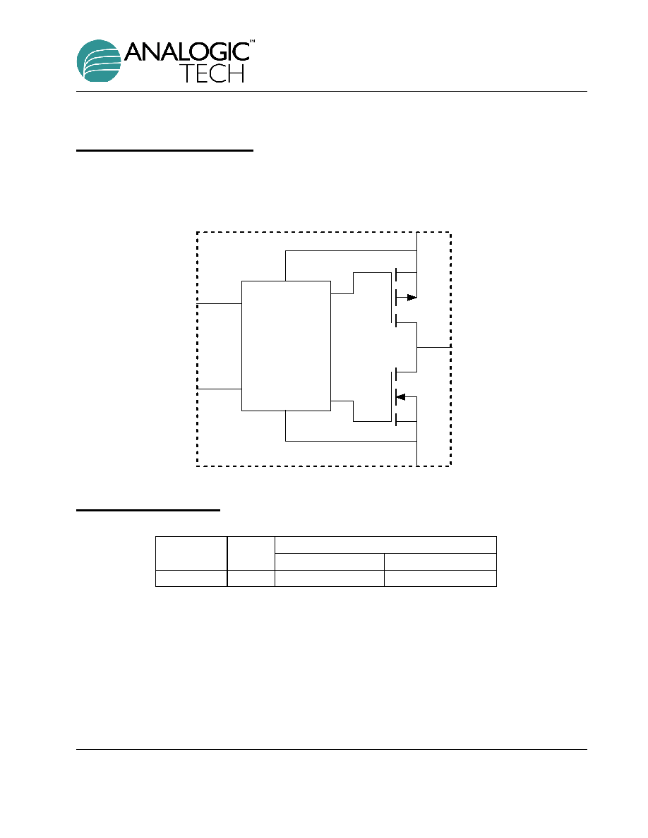
Functional Block Diagram
Ordering Information
Part Number
Package Marking
Bulk
Tape and Reel
SOT-23-5
N/A
AAT4900IGV-T1
8-3
Control Logic
and
Shoot-through
Protection
CLK
EN
IN
OUT
GND

AAT4900
Buffered Power Half-Bridge
Advanced Analogic Technologies, Inc.
1250 Oakmead Pkwy, Suite 310, Sunnyvale, CA 94086
(408)524-9684 Fax (408)524-9689
4900.2000.9.0.71
This page intentionally left blank
8-4