General Description
The AAT9125 30V N-Channel Power MOSFET is a
member of AnalogicTech's TrenchDMOSTM prod-
uct family. Using the ultra-high density proprietary
TrenchDMOS technology, this product demon-
strates high power handling and small size.
Applications
∑
DC-DC converters for mobile CPUs
∑
Battery-powered portable equipment
∑
High power density switch-mode supplies
∑
Point-of-use Power Supplies
Features
∑
V
DS(MAX)
= 30V
∑
I
D(MAX)
= 12.5A @ 25∞C
∑
Low R
DS(ON)
:
∑
9 m
@V
GS
= 10V
∑
14 m
@ V
GS
= 4.5V
SOP8 Package
D
D
D
D
S
S
S
G
Top View
1
2
3
4
8
7
6
5
AAT9125
30V N-Channel Power MOSFET
Absolute Maximum Ratings
(T
A
=25∞C unless otherwise noted)
Thermal Characteristics
Note 1: Mounted on 1" x 1" FR4 Copper Board, 10 sec pulse width
Symbol
Description
Value
Units
R
JA
Typical Junction-to-Ambient
1
50
∞C/W
R
JC
Typical Junction-to-Case
25
∞C/W
Symbol
Description
Value
Units
V
DS
Drain-Source Voltage
30
V
V
GS
Gate-Source Voltage
±20
I
D
Continuous Drain Current @ T
J
=150∞C
1
T
A
= 25∞C
±12.5
T
A
= 70∞C
±10
A
I
DM
Pulsed Drain Current
±52
I
S
Continuous Source Current (Source-Drain Diode)
1
2.25
P
D
Maximum Power Dissipation
1
T
A
= 25∞C
2.5
W
T
A
= 70∞C
1.6
T
J
, T
STG
Operating Junction and Storage Temperature Range
-55 to 150
∞C
Preliminary
Information
9125.2001.12.0.9
1
PWMSwitch
TM

Electrical Characteristics
(T
J
=25∞C unless otherwise noted)
Note 2: Pulse test: Pulse Width = 300µs
Note 3: Guaranteed by design. Not subjected to production testing.
Symbol
Description
Conditions
Min
Typ
Max
Units
DC Characteristics
BV
DSS
Drain-Source Breakdown Voltage V
GS
=0V, I
D
=250µA
30
V
R
DS(ON)
Drain-Source ON-Resistance
2
V
GS
=10V, I
D
=12A
7.5
9
m
V
GS
=4.5V, I
D
=10A
11.5
14
I
D(ON)
On-State Drain Current
2
V
GS
=10V ,V
DS
=5V (Pulsed)
52
A
V
GS(th)
Gate Threshold Voltage
V
GS
=V
DS
, I
D
=250µA
1.0
V
I
GSS
Gate-Body Leakage Current
V
GS
=±20V, V
DS
=0V
±100
nA
I
DSS
Drain Source Leakage Current
V
GS
=0V,V
DS
=30V
1
µA
V
GS
=0V,V
DS
=30V, T
J
=55∞C
5
g
fs
Forward Transconductance
2
V
DS
=15V, I
D
=12.5A
30
S
Dynamic Characteristics
3
Q
G
Total Gate Charge
V
DS
=15V, I
D
=12.5A, V
GS
=5V
31
50
nC
Q
GT
Total Gate Charge
V
DS
=15V, I
D
=12.5A, V
GS
=10V
60
100
nC
Q
GS
Gate-Source Charge
V
DS
=15V, I
D
=12.5A, V
GS
=10V
10
nC
Q
GD
Gate-Drain Charge
V
DS
=15V, I
D
=12.5A, V
GS
=10V
9
nC
t
D(ON)
Turn-ON Delay
V
DD
=15V, V
GS
=10V, R
D
=1.2
, R
G
=6
20
35
ns
t
R
Turn-ON Rise Time
V
DD
=15V, V
GS
=10V, R
D
=1.2
, R
G
=6
14
30
ns
t
D(OFF)
Turn-OFF Delay
V
DD
=15V, V
GS
=10V, R
D
=1.2
, R
G
=6
100
160
ns
t
F
Turn-OFF Fall Time
V
DD
=15V, V
GS
=10V, R
D
=1.2
, R
G
=6
38
80
ns
Source-Drain Diode Characteristics
V
SD
Source-Drain Forward Voltage
2
V
GS
=0, I
S
=2.25A
1.1
V
I
S
Continuous Diode Current
T
A
=25∫C
2.25
A
AAT9125
30V N-Channel Power MOSFET
2
9125.2001.12.0.9

Typical Characteristics
(T
J
= 25∫C unless otherwise noted)
Gate Charge Characteristics
0
2
4
6
8
10
0
10
20
30
40
50
60
Gate Charge (nC)
Gate Voltage (V)
Source to Drain Voltage
0.1
1
10
100
0.4
0.6
0.8
1
1.2
V
SD
(V)
I
SD
(A)
Transfer
0
10
20
30
40
50
0
1
2
3
4
5
V
G
(V)
I
D
(A)
V
G
=V
D
R
DS(ON)
vs. V
G
0
10
20
30
40
50
0
2
4
6
8
10
V
G
(V)
R
DS(ON)
(mW)
10A
5A
15A
Normalized R
DS(ON)
0
0.5
1
1.5
2
2.5
3
0
10
20
30
40
50
I
D
(A)
R
DS(ON)
/
R
DS(ON)
at gate = 10 V
10 V
3.5 V
5 V
4 V
4.5 V
6 V
Forward Characteristics
0
10
20
30
40
50
0
1
2
3
4
5
V
D
(V)
I
D
(A)
3.5V
2V
10V
3V
4V
4.5V
6V 5V
AAT9125
30V N-Channel Power MOSFET
9125.2001.12.0.9
3

Ordering Information
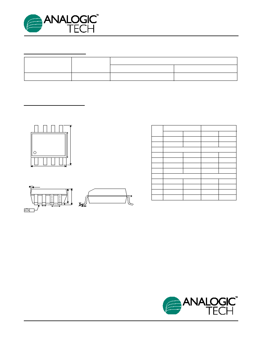
Package Information
SOP-8
E
b
e
H
D
A1
A
A2
7 (4x)
c
L
y
Q
Package
Marking
Part Number
Bulk
Tape and Reel
SOP-8
AAT9125IAS-B1
AAT9125IAS-T1
AAT9125
30V N-Channel Power MOSFET
4
9125.2001.12.0.9
Advanced Analogic Technologies, Inc.
1250 Oakmead Parkway, Suite 310, Sunnyvale, CA 94086
Phone (408) 524-9684
Fax (408) 524-9689
Dim
Millimeters
Inches
Min
Max
Min
Max
A
1.35
1.75
0.053
0.069
A1
0.10
0.25
0.004
0.010
A2
1.45
0.057
B
0.33
0.51
0.013
0.020
C
0.19
0.25
0.007
0.010
D
4.80
5.00
0.189
0.197
E
3.80
4.00
0.150
0.157
e
1.27
0.050
H
5.80
6.20
0.228
0.244
L
0.40
1.27
0.016
0.050
Y
0.00
0.10
0.000
0.004
1
0∞
8∞
0∞
8∞
Note:
1. PACKAGE BODY SIZES EXCLUDE MOLD FLASH
PROTRUSIONS OR GATE BURRS.
2. TOLERANCE 0.1000mm (4mil) UNLESS
OTHERWISE SPECIFIED
3. COPLANARITY: 0.1000mm
4. DIMENSION L IS MEASURED IN GAGE PLANE.
5. CONTROLLING DIMENSION IS MILLIMETER;
CONVERTED INCH DIMENSIONS ARE NOT
NECESSARILY EXACT.


