 | –≠–ª–µ–∫—Ç—Ä–æ–Ω–Ω—ã–π –∫–æ–º–ø–æ–Ω–µ–Ω—Ç: aTS75M8T | –°–∫–∞—á–∞—Ç—å:  PDF PDF  ZIP ZIP |
Preliminary Specification
© Andigilog, Inc. 2001
www.andigilog.com
Sep 2001 -rev.5.84
1
L
OW
-V
OLTAGE
2-W
IRE
D
IGITAL
T
EMPERATURE
S
ENSOR
With Thermal Alarm
aTS75
P
RODUCT
S
PECIFICATION
Product Description
The aTS75 is a high-precision CMOS temperature sensor
with a Delta-Sigma temperature-to-digital converter and a
SMBus compatible serial digital interface. The aTS75 is
typically accurate to ±2∞C over the full temperature range of
-
40∞C to 125∞C and to ±1∞C over the range of 0∞C to
100∞C. The aTS75 provides digital temperature data with
9- to 12-bit resolution. The default resolution is 9-bits, but
for applications requiring higher resolution, the user can
program the aTS75 to provide 10-, 11-, or 12-bit data.
The aTS75 features a thermal alarm function with a user-
programmable trip temperature and turn-off temperature.
This alarm can operate in two modes -- interrupt mode and
comparator mode -- which allows flexibility for many types
of applications.
The aTS75 is available in SOP-8 and MSOP-8 surface
mount packages.
Features
User Configurable to 9-, 10-, 11-, or 12-bit Resolution
Precision Calibrated to ±1∞C from 0∞C to 100∞C Typical
Temperature Range: -40∞C to 125∞C
Low Operating Current (less than 250
µ
A)
Low Self Heating (0.2∞C max in still air)
Operating Voltage Range: 2.7V to 5.5V
Applications
Battery Management
FAX Management
Printers
Portable Medical Instruments
HVAC
Power Supply Modules
Disk Drives
Computers
Automotive
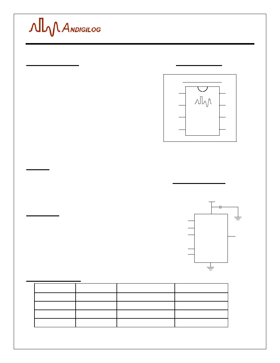
Pin Configuration
Application Diagram
Ordering Information
Part Number
Package
Temperature Range
How Supplied
aTS75D8
8-Lead SOP
-40∞C to 125∞C
98 units/tube
aTS75D8T
8-Lead SOP
-40∞C to 125∞C
2500 units Tape & Reel
aTS75M8
8-Lead MSOP
-40∞C to 125∞C
50 units/tube
aTS75M8T
8-Lead MSOP
-40∞C to 125∞C
4000 units Tape & Reel
1
2
3
4
5
6
7
8
GND
O.S.
SCL
SDA
V
DD
A0
A1
A2
SOP8 and MSOP8
aTS75
2.7V to 5.5V
aTS75
8 Pin
Configuration
SMBus
Interface
User
Programmable
Address
A0
A1
A2
SDA
SCL
O.S.
8
7
6
5
1
2
4
3

Preliminary Specification
© Andigilog, Inc. 2001
www.andigilog.com
Sep 2001 -rev.5.84
2
aTS75
Absolute Maximum Ratings
1
Parameter
Rating
Supply Voltage
+7V
Output Voltage
V
CC
+ 0.5V
Output Current
10mA
Storage Temperature Range
-60
∞
C to +150
∞
C
Lead Soldering Temperature
220
∞
C
Human Body Model
2000 V
ESD
2
Machine Model
250 V
Electrical Characteristics
3
(-40∞C
T
A
+125∞C, VCC=5.0V unless otherwise noted. Specifications subject to change without notice)
Parameter
Symbol
Conditions
Min
Typ
Max
Units
Specified Temperature Range
T
MIN
, T
MAX
-40
--
+125
∞C
Temperature Conversion Time
4
90
ms
Accuracy
5
T
A
= 0∞C
T
A
=+25∞C
T
A
=+100∞C
T
A
= -40∞C (T
MIN
)
T
A
=+125∞C (T
MAX
)
-1
-1
-1
-3
-3
--
--
--
--
--
+1
+1
+1
+3
+3
∞C
∞C
∞C
∞C
∞C
Logic Electrical Characteristics
(T
A
= 25 ∞C, V
DD
= 5V unless otherwise noted)
Parameter
Symbol
Conditions
Min
Typ
Max
Units
Min Input Voltage Logic High
V
IH
V
DD
X 0.7
V
DD
+ 0.5
V
Max Input Voltage Logic Low
V
IL
-0.3
V
DD
X 0.3
V
Max Output Voltage Logic Low
V
OL
V
DD
= 5V, I
OL
= -3mA
V
DD
= 3V, I
OL
= -1.5mA
0.36
0.36
V
Quiescent Supply Current
I
DD
Interface Inactive
R/W Activity on SDA
220
350
250
500
µA
Shutdown Current
I
DD-SD
Interface Inactive
R/W Activity on SDA
0.15
83
1
150
µA
Input Leakage Current
I
IN
V
IN
= 0V or 5V, T
A
= 25 ∞C
-40∞C < T
A
< 125 ∞C
±0.1
±1.0
µA
Output Sink Current
I
OL
T
A
= 25 ∞C, V
OL
= 0.4V
3
mA
Output Leakage Current
I
LEAK
V
OH
= 5V, V
DD
= 0V
0.001
5
µA
Output Transition Time
t
F
C
L
= 400pF, I
OL
= -3mA
250
ns
Input Capacitance
C
IN
All Digital Inputs
20
pF
Notes:
1. Absolute maximum ratings are limits beyond which operation may cause permanent damage to the device. These are
stress ratings only; functional operation at or above these limits is not implied.
2. Human Body Model: 100pF capacitor discharged through a 1.5k
resistor into each pin. Machine Model: 200pF capacitor
discharged directly into each pin.
3. These specifications are guaranteed only for the test conditions listed.
4. This specification only indicates how often temperature information is updated to the Temperature Register. The aTS75
can be read at any time without interrupting the temperature conversion process.
5. Accuracy (expressed in ∞C) = Difference between the aTS75 output temperature and the measured temperature.

Preliminary Specification
© Andigilog, Inc. 2001
www.andigilog.com
Sep 2001 -rev.5.84
3
aTS75
Serial Port Timing
(T
A
= 25 ∞C, V
DD
= 5V unless otherwise noted)
Parameter
Symbol
Conditions
Min
Typ
Max
Units
SCL Clock Period
t
SCL
1.0
100
µ
s
SCL Clock Transition Time
t
T:LH
, t
T:HL
300
ns
SCL Clock Low Period
t
LOW
0.470
µ
s
SCL Clock High Period
t
HIGH
0.400
50
µ
s
Bus free time between a Stop and a
new Start Condition
t
BUF
1.0
µ
s
Data in Set-Up to SCL High
t
SU:DAT
100
ns
Data Out Stable after SCL Low
t
HD:DAT
0
ns
SCL Low Set-up to SDA Low
(Repeated Start Condition)
t
SU:STA
100
ns
SCL High Hold after SDA Low (Start
Condition)
t
HD:STA
100
ns
SDA High after SCL High (Stop
Condition)
t
SU:STO
100
ns
Time in which aTS77 must be
operational after a power-on reset
t
POR
500
ms
Pin Descriptions
Pin #
Name
Direction
Description
1
SDA
Input/Output
Serial Data--Open drain I/0-data pin for two-wire interface.
2
SCL
Input
Serial Clock--Clock for 2-wire serial interface.
3
O.S.
Output
Over-Limit Signal--Open drain thermostat output that indicates if the
temperature has exceeded user-programmable limits
4
GND
Supply
Ground
5, 6,7
A0, A1, A2
Input
Address LSBs--User selectable address pins for the 3 lsbs of the
serial interface address.
8
V
DD
Supply
Supply Voltage
SDA
Data In
t
HD:STA
t
SCL
t
SU:STO
t
SU:DAT
t
HD:DAT
SCL
SDA
Data Out
SCL
10%
10%
90%
t
T:LH
t
T:HL
t
LOW
t
HIGH
t
BUF
t
SU:STA
90%

Preliminary Specification
© Andigilog, Inc. 2001
www.andigilog.com
Sep 2001 -rev.5.84
4
aTS75
Basic Operation
The aTS75 temperature sensing circuitry continuously
produces an analog voltage that is proportional to the
device temperature. At regular intervals the aTS75
converts the analog voltage to a two's complement digital
value, which is placed into the temperature register.
The aTS75 has an SMBus compatible digital serial
interface which allows the user to access the data in the
temperature register at any time. In addition, the serial
interface gives the user easy access to all other aTS75
registers to customize operation of the device.
The aTS75 temperature-to-digital conversion can have 9-,
10-, 11-, or 12-bit resolution as selected by the user,
providing 0.5
∞
C, 0.25
∞
C, 0.125
∞
C, and 0.0625
∞
C
temperature resolution, respectively. At power-up the
default conversion resolution is 9-bits. The conversion
resolution is controlled by the R0 and R1 bits in the
Configuration Register.
Table 1 gives examples of the relationship between the
output digital data and the external temperature. The 9-bit,
10-bit, 11-bit and 12-bit columns in Table 1 indicate the
right-most bit in the output data stream that can contain
temperature information for each conversion accuracy.
Since the output digital data is in two's-complement format,
the most significant bit of the temperature is the "sign" bit.
If the sign bit is a zero, the temperature is positive and if
the sign bit is a one, the temperature is negative.
The aTS75 has a Shutdown Mode that reduces the
operating current of the aTS75 to 150nA. This mode is
controlled by the SD bit in the configuration register.
Power Up Default Conditions
The ATS75 always powers up in the following default state:
ß
Thermostat mode: Comparator Mode
ß
O.S. polarity: active low
ß
Fault tolerance: 1 fault (i.e., F0=0 and F1=0 in the
Configuration Register)
ß
T
OS
= 80
∞
C
ß
T
HYST
= 75
∞
C
ß
Register pointer: 00 (Temperature Register)
ß
Conversion resolution: 9 bits (i.e., R0=0 and R1=0
in the Configuration Register)
After power up these conditions can be reprogrammed via
the serial interface. Refer to the Serial Data Bus Operation
section to for aTS75 programming instructions.
Thermal Alarm Function
The aTS75 thermal alarm function provides user
programmable thermostat capability and allows the aTS75
to function as a standalone thermostat without using the
serial interface. The Over-Limit Signal (O.S.) output is the
alarm output. This signal is an open drain output, and at
power-up this pin is configured with active-low polarity.
Table 1. Relationship Between Temperature and Digital
Output
Temperature
Digital Output
Sign Bit
Number of bits
used by
conversion
resolution
9
-
bit
10
-
bit
11
-
bit
12
-
bit
Always
zero
12-Bit Resolution
0000
11-Bit Resolution
0
0000
10-Bit Resolution
0
0
0000
All Temperatures
9-Bit Resolution
0 0
0
0000
+125
∞
C
0 111
1101
0
0 0
0
0000
+100.0625
∞
C
0 110
0100
0
0 0
1
0000
+50.125
∞
C
0 011
0010
0
0 1
0
0000
+12.25
∞
C
0 000
1100
0
1 0
0
0000
0
∞
C
0 000
0000
0
0 0
0
0000
-20.5
∞
C
1 110
1011
1
0 0
0
0000
-33.25
∞
C
1 101
1110
1
1 0
0
0000
-45.0625
∞
C
1 101
0010
1
1 1
1
0000
-55
∞
C
1 100
1001
0
0 0
0
0000
The O.S. polarity is controlled by the POL bit in the
Configuration Register. The user-programmable upper
trip-point temperature for the thermal alarm is stored in the
T
OS
Register, and the user-programmable hysteresis
temperature (i.e., the lower trip point) is stored in the T
HYST
Register.
The thermal alarm has two modes of operation:
Comparator Mode and Interrupt Mode. At power-up the
default is Comparator Mode. The alarm mode is controlled
by the CMP/INTR bit in the Configuration Register.
Fault Tolerance
In either mode the alarm "fault tolerance" setting plays a
role in determining when the O.S. output will be activated.
Fault tolerance refers to the number of consecutive times
an error condition must be detected before the user is
notified. Higher fault tolerance settings can help eliminate
false alarms caused by noise in the system. The alarm
fault tolerance is controlled by bits F0 and F1 in the
Configuration Register. These bits can be used to set the
fault tolerance to 1, 2, 4 or 6 as shown in Table 4. At
power-up, these bits both default to 0 ( fault tolerance = 1).

Preliminary Specification
© Andigilog, Inc. 2001
www.andigilog.com
Sep 2001 -rev.5.84
5
aTS75
Comparator Mode
In Comparator Mode, each time an temperature-to-
digital(T-to-D) temperature conversion occurs, the new
digital temperature is compared to the value stored in the
T
OS
and T
HYST
Registers. If a fault tolerance number of
consecutive temperature measurements are greater than
the value stored in the T
OS
Register, the O.S. output will be
activated. For example, if bits F1 and F0 are equal to "10"
(fault tolerance = 4), four consecutive temperature
measurements must exceed T
OS
to activate the O.S.
output. Once the O.S output is active, it will remain active
until the first time the measured temperature drops below
the temperature stored in the T
HYST
Register. The
operation of the alarm in Comparator Mode with fault
tolerance=2 is illustrated in Figure 1.
Interrupt Mode
In Interrupt Mode the O.S. output will first become active
after a fault tolerance number of consecutive temperature
measurements exceed the value stored in the T
OS
Register
(similar to Comparator Mode). Once O.S. is active, it can
only be cleared by a user read from any of the aTS75
registers (Temperature, Configuration, T
OS
, or T
HYST
) or by
putting the aTS75 into Shutdown Mode (i.e., by setting the
shutdown bit in the Configuration Register to "1"). Once
cleared, the O.S. output can only be activated again by a
fault tolerance number of consecutive temperature
measurements that are lower than the value stored in
T
HYST
. Again, once it is activated the O.S. output can only
be deactivated by a user read or shutdown. Thus, in
Interrupt Mode the activate/clear cycle for O.S. has the
following pattern: temperature > T
OS
, clear,
temperature < T
HYST
, clear, temperature > T
OS
, clear, etc.
The operation of the alarm in Interrupt Mode with fault
tolerance=2 is also illustrated in Figure 1.
Figure 1. Thermal Alarm Operation in Comparator and Interrupt Modes
For this example:
Fault Tolerance = 2
Output Polarity = Active Low
Read (or Shutdown)
T
OS
T
HYST
Temperature-to-Digital
Conversion
O.S. (Comparator Mode)
O.S. (Interrupt Mode)