
Stereo 2.8W Audio Power Amplifier with DC Volume Control
and Selectable Gain
Copyright
ANPEC Electronics Corp.
Rev. A.
7 -
Mar
.,
2003
APA4835
www.anpec.com.tw
1
ANPEC reserves the right to make changes to improve reliability or manufacturability without notice, and advise
customers to obtain the latest version of relevant information to verify before placing orders.
Features
General Description
Applications
Pin Description
∑
Operating Voltage : 3.3V to 5V
∑
Stereo switchable bridged/single-ended
power amplifiers
∑
DC Volume Control Interface , 0dB to ≠105dB
∑
Low Supply Current , I
DD
= 13mA at Stereo BTL
∑
Low Shutdown Current , I
DD
= 0.7µA
∑
Bridge-Tied Load (BTL) or Single-Ended-(SE)
Modes Operation
∑
Output Power at 1% THD+N , V
DD
=5V
≠
2.2W/Ch (typ) into a 3
Load
≠
2.0W/Ch (typ) into a 4
Load
≠
1.2W/Ch (typ) into a 8
Load
∑
Output Power at 10% THD+N , V
DD
=5V
≠
2.8W/Ch (typ) into a 3
Load
≠
2.3W/Ch (typ) into a 4
Load
≠
1.5W/Ch (typ) into a 8
Load
∑
Single-ended mode at 1.0% THD+N
≠
95mW/Ch (typ) into 32
Load
∑
Depop Circuitry Integrated
∑
System Beep Detect
∑
Thermal shutdown protection circuitry
∑
High supply voltage ripple rejection
∑
Low Crossover Distortion
∑
PC99 Compliant
∑
28-pin TSSOP-P (with enhanced thermal pad)
power package available
∑
Notebook and Desktop Computers
∑
Multimedia Monitors
∑
Portable Applications
The APA4835 is a monolithic integrated circuit , which
provides DC volume control , and a stereo bridged
audio power amplifiers capable of producing 2.8W
(2.2W) into 3
with less than 10% (1.0%) THD+N.
APA4835 includes a DC volume control , stereo
bridge-tied and single-ended audio power amplifiers
, stereo docking outputs , and a selectable gain con-
trol , that makes it optimally fittable for notebook PC
, multimedia monitors , and other portable
applications. The attenuator range of the volume
control in APA4835 is from 0dB (DC_Vol=0.7V
DD
) to
≠105dB (DC_Vol=0V) with 32 steps. Both of the
depop circuitry and the thermal shutdown protection
circuitry are integrated in APA4835 , that reduces
pops and clicks noise during power up or shutdown
mode operation , and protects the chip from being
destroyed by over temperature failure. To simplify
the audio system design , APA4835 combines a ste-
reo bridge-tied loads (BTL) mode for speaker drive
and a stereo single-end (SE) mode for headphone
drive into a single chip , where both modes are easily
switched by the SE/BTL input control pin signal. Be-
sides the low supply current design to increase the
efficiency of the amplifiers , APA4835 also features a
shutdown function which keeps the supply current
only 0.7µA (typ).
SHUTDOWN
GND
V
DD
GND
HP Sense
BYPASS
Right Dock
Gain Select
Mode
Mute
DC Vol
Right In
Beep In
Left In
Left Dock
GND
10
1
2
3
4
5
6
7
8
9
11
12
13
14
Right Out +
V
DD
Right Out -
Right Gain 2
Right Gain 1
GND
Left Gain 1
Left Gain 2
Left Out -
GND
V
DD
Left Out +
28
27
26
25
24
23
22
21
20
19
18
17
16
15
Copyright
ANPEC Electronics Corp.
Rev. A.
7 -
Mar
.,
2003
APA4835
www.anpec.com.tw
2
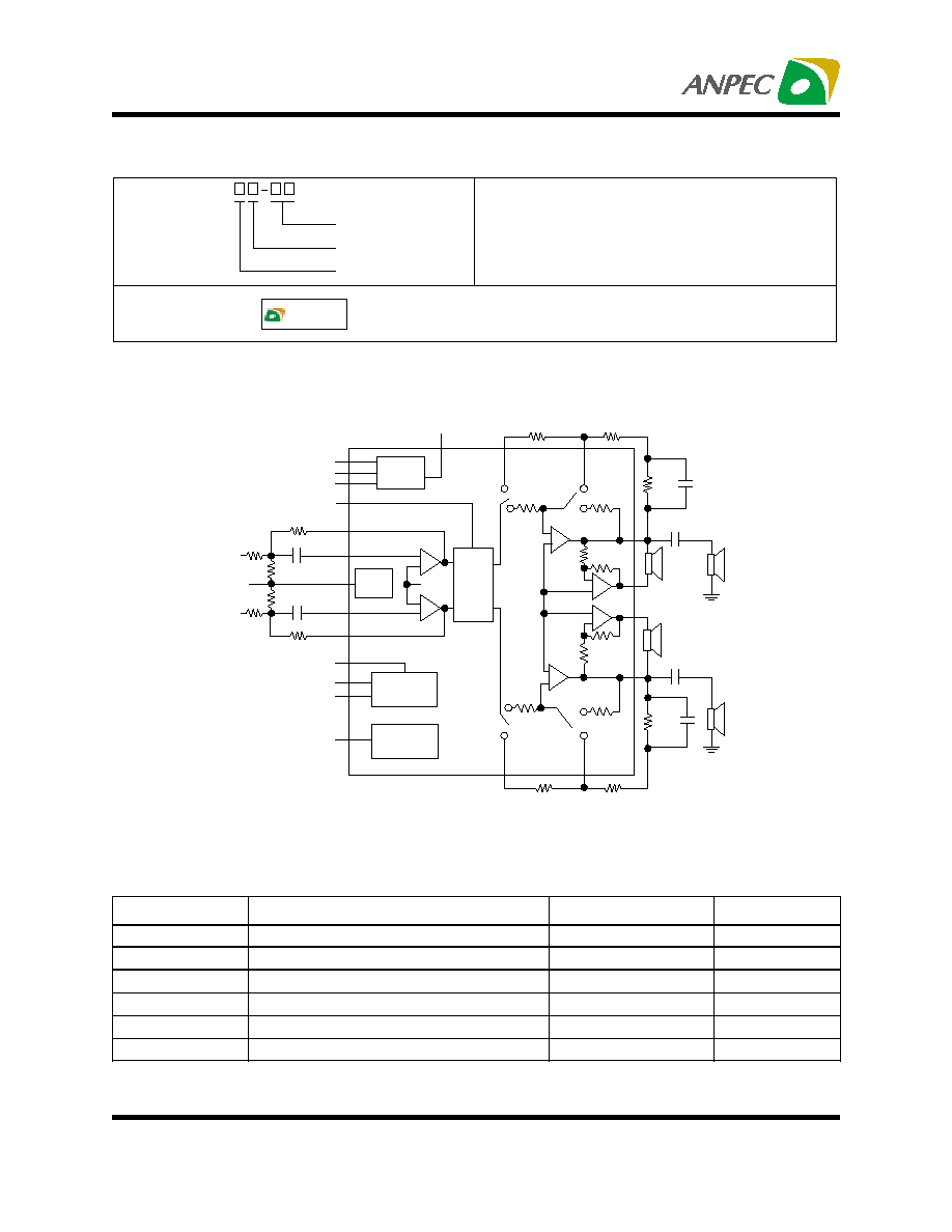
Block Diagram
(Over operating free-air temperature range unless otherwise noted.)
Symbol
Parameter
Rating
Unit
V
DD
Supply Voltage
6
V
T
A
Operating Ambient Temperature Range
-40 to 85
∞
C
T
J
Maximum Junction Temperature
Internally limited*
1
∞
C
T
STG
Storage Temperature Range
-65 to +150
∞
C
T
S
Soldering Temperature,10 seconds
260
∞
C
V
ESD
Electrostatic Discharge
-2000 to 2000*
2
V
Absolute Maximum Ratings
Note :*1. APA4835 integrates internal thermal shutdown protection when junction temperature ramp up to 150∞C.
*2. Human body model : C=100pF, R=1500
, 3 positive pulses plus 3 negative pulses
Ordering Information
P a c k a g e C o d e
R : T S S O P -P
T e m p . R a n g e
I : -4 0 to 8 5 C
H a n d lin g C o d e
T U : T u b e T R : T a p e & R e e l
A P A 48 3 5
H a n d lin g C o d e
T e m p . R a n g e
P a c k a g e C o d e
∞
A P A 4 8 3 5 R :
A P A 4 8 3 5
X X X X X
X X X X X - D a te C o d e
Mode
Control
Mode
Mute
HP Sense
Volume
Control
32 steps
Beep
Detect
-
+
-
+
Power
Management
Click and Pop
Suppression
Circuitry
-
+
-
+
-
+
Internal gain select
Left Dock
20K
20K
20K
10K
10K
- Left Out
20K
20K
+ Right Out
- Right Out
0.068
µ
F
20K
10K
20K
20K
10K
0.068
µ
F
20K
20K
Right Dock
Shutdown
V
DD
GND
Bypass
Bias
Left In
0.33
µ
F
Right In
0.33
µ
F
20K
200K
200K
20K
Beep In
+ Left Out
-
+
DC Vol Control
20K
20K
Copyright
ANPEC Electronics Corp.
Rev. A.
7 -
Mar
.,
2003
APA4835
www.anpec.com.tw
3
Electical Characteristics
Electrical Characteristics for Volume Attenuators
The following specifications apply for V
DD
= 5V. Limits apply for T
A
= 25∞C
Electrical Characteristics for Entire IC
The following specifications apply for V
DD
= 5V unless otherwise noted. Limits apply for T
A
= 25∞C
Electrical Characteristics for BTL Mode Operation
The following specifications apply for V
DD
= 5V unless otherwise noted. Limits apply for T
A
= 25∞C
APA4835
Symbol
Parameter
Test Conditions
Min.
Typ.
Max.
Unit
V
DD
Supply Voltage
3.3
5.5
V
I
DD
Quiescent Power Supply
Current
V
IN
=0V, I
O
=0A
13
25
mA
I
SD
Shutdown Current
V
PIN 2
= V
DD
0.7
2.0
µ
A
V
IH
SE/BTL High Input Voltage
4
V
V
IL
SE/BTL Low Input Voltage
0.8
V
APA4835
Symbol
Parameter
Test Conditions
Min.
Typ.
Max.
Unit
Gain with V
PIN 7
=5V
±0.5
C
RANGE
Attenuator Range
Attenuation with V
PIN 7
=0V
-90
-105
dB
V
PIN 5
=5V, Bridged Mode
-88
A
M
Mute Attenuation
V
PIN 5
=5V, Single-Ended Mode
-88
dB
APA4835
Unit
Symbol
Parameter
Test Conditions
Typ.
V
OS
Output Offset Voltage
V
IN
=0V
5
mV
THD=1%, f=1kHz
R
L
=3
R
L
=4
R
L
=8
2.2
2.0
1.2
P
O
Output Power
THD=10%, f=1kHz
R
L
=8
1.5
W
Thermal Characteristics
Symbol
Parameter
Rating
Unit
R
THJA
Thermal Resistance from Junction to Ambient in Free Air
TSSOP-P*
TSSOP-P**
60
35
∞C/W
*5in
2
printed circuit board with 2oz trace and copper pad through 12 25mil diameter vias. The thermal pad on the TSSOP_P package
without solder on the printed circuit board.
**5in
2
printed circuit board with 2oz trace and copper pad through 12 25mil diameter vias. The thermal pad on the TSSOP_P package
with solder on the printed circuit board.

Copyright
ANPEC Electronics Corp.
Rev. A.
7 -
Mar
.,
2003
APA4835
www.anpec.com.tw
4
APA4835
Symbol
Parameter
Test Conditions
Typ.
Unit
V
OS
Output Offset Voltage
V
IN
=0V
5
mV
THD=1%,
f=1kHz, R
L
=32
95
P
O
Output Power
THD=10%,
f=1kHz, R
L
=32
100
mW
A
V
= 1 , V
OUT
=1V
RMS
, f=1kHz, R
L
=1k
0.01
%
THD+N Total Harmonic Distortion
plus Noise
P
O
=75mW, R
L
=32
, A
V
= 1, f=1kHz
0.005
%
PSRR Power Supply Rejection
Ratio
V
RIPPLE
=200mV
RMS
, f=120Hz, C
B
=2.2
µ
F
58
dB
X
TALK
Channel Separation
f=1kHz , C
B
=2.2
µ
F
95
dB
SNR
Signal-to-Noise Ratio
P
O
=75mW, R
L
=32
, A-Wtd Filter
102
dB
V
N
Output Noise Voltage
R
L
=1k
, A-Wtd Filter
40
uV
APA4835
Unit
Symbol
Parameter
Test Conditions
Typ.
A
VD
=2, 20Hz<f<20kHz
R
L
=4
, P
O
=1W
R
L
=8
, P
O
=1W
0.2
0.15
THD+N
Total Harmonic Distortion + Noise
R
L
=32
, P
O
=340mW
0.1
%
PSRR
Power Supply Rejection Ratio
V
RIPPLE
=200mV
Rms
, R
L
=8
C
B
=2.2
µ
F, f=120Hz
74
dB
X
TALK
Channel Separation
f=1kHz , C
B
=2.2
µ
F
95
dB
SNR
Signal-to-Noise Ratio
V
DD
=5V, P
O
=1.1W, R
L
=8
,A-Wtd
Filter
95
dB
V
N
Output Noise Voltage
R
L
=8
,A-Wtd Filter
30
uV
Electical Characteristics (Cont.)
Electrical Characteristics for SE Mode Operation
The following specifications apply for V
DD
= 5V unless otherwise noted. Limits apply for T
A
= 25∞C
Pin Description
Pin
Name
No
I/O
Description
GND
1, 8, 14, 20,
23
Ground connection for circuitry.
Shutdown
2
I
Shutdown mode control signal input, place entire IC in shutdown mode when held high, Idd=0.7uA
Gain Select
3
I
Gain select input pin
Mode
4
I
Mode select input pin
Mute
5
I
Mute control input pin
Electrical Characteristics for BTL Mode Operation (Cont.)
The following specifications apply for V
DD
= 5V unless otherwise noted. Limits apply for T
A
= 25∞C

Copyright
ANPEC Electronics Corp.
Rev. A.
7 -
Mar
.,
2003
APA4835
www.anpec.com.tw
5
Pin
Name
No
I/O
Description
VDD
6, 16, 27
Supply voltage input pin
DC_Vol
7
I
Volume control function input pin.
Right Dock
9
O Right docking output pin
Right In
10
I
Right channel audio input pin
Beep In
11
I
Beep signal input pin
Left In
12
I
Left channel audio input pin
Left Dock
13
O Right docking output pin
Left Out +
15
O Left channel positive output pin
Left Out -
17
O Left channel negative output pin
Left Gain 2
18
Connect pin 2 of the external gain setting resistor for left channel
Left Gain 1
19
Connect pin 1 of the external gain setting resistor for left channel
HP Sense
21
I
Headphone sense control pin
Bypass
22
Bypass pin
Right Gain 1
24
Connect pin 1 of the external gain setting resistor for right channel
Right Gain 2
25
Connect pin 2 of the external gain setting resistor for right channel
Right Out -
26
O Right channel negative output pin
Right Out +
28
O Right channel positive output pin
Truth Table for Logic Inputs
Mute
Mode
HP Sense
DC Vol. Control Bridged Output Single-Ended
0
0
0
Fixed Level
Vol. Fixed
-
0
0
1
Fixed Level
Muted
Vol. Fixed
0
1
0
Adjusted
Vol. Changes
-
0
1
1
Adjusted
Muted
Vol. Changed
1
◊
◊
-
Muted
Muted
Pin Description