
Copyright
ANPEC Electronics Corp.
Rev. A.4 - July., 2002
APC558
www.anpec.com.tw
1
ANPEC reserves the right to make changes to improve reliability or manufacturability without notice, and advise
customers to obtain the latest version of relevant information to verify before placing orders.
Dual Operational Amplifier
Features
Applications
General Description
Ordering and Marking Information
∑∑
∑∑
∑
Power Supply Range :
∑
Signal Supply : 3V to 20V
∑
Dual Supply :
±
1.5V to
±
10V
∑∑
∑∑
∑
Large DC Voltage Gain : 100dB
∑∑
∑∑
∑
Large Output Swing : 0V ~ V
DD
- 1.5V
∑∑
∑∑
∑
Bandwidth(unity gain) : 2MHz
∑∑
∑∑
∑
Internally Frequency Compensated for Unity
Gain
∑∑
∑∑
∑
Low Input Offset Voltage : 1mV
∑∑
∑∑
∑
Amplifiers
∑∑
∑∑
∑
Filters
∑∑
∑∑
∑
Analog Circuit
P a ck a ge C o d e
J : P D IP K : S O P -8
O : T S S O P -8
T e m p . R a ng e
C : 0 to 7 0 C
H a n dlin g C o d e
T U : T ub e
T R : T ap e & R e el
L ea d F ree C o d e
L : L ea d F ree D e vic e B lan k : O rigin al D e vic e
A P C 5 5 8
H a n dlin g C o d e
T e m p . R a ng e
P a ck a ge C o d e
∞
A P C 5 5 8 J :
A P C 5 5 8
XXXXX
XXXXX - D a te C od e
A P C 5 5 8 K /O :
A P C 5 5 8
XXXXX
XXXXX - D a te C od e
L ea d F ree C o d e
The APC558 consists of two independent, high gain,
internally frequency compensated operational am-
plifiers which were designed specifically to operate
from a single power supply up to 20 volts. Operation
from dual power supplies is also possible and the
power supply current drain is essentially indepen-
dent of the magnitude of the power supply voltage.
Application areas include transducer amplifiers, DC
gain blocks and all the conventional OP amplifier
circuits which can be more easily implemented in
single power supply systems. (For example, the
APC558 can be directly operated from the standard
+5V power supply voltage which is normally used in
digital systems.)
Copyright
ANPEC Electronics Corp.
Rev. A.4 - July., 2002
APC558
www.anpec.com.tw
2
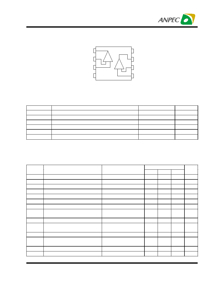
Block Diagram
Output B
Inverting Input B
1
2
3
4
5
6
7
8
Output A
Inverting Input A
Non-inverting Input B
V
D D
+
V
D D
-
B
-
+
A
- +
Non-inverting Input A
Absolute Maximum Ratings
T
A
= 25
∞
C
Electrical Characteristics
V
DD
=
±
10V, T
A
= 25
∞
C
APC558
Symbol
Parameter
Test Conditions
Min.
Typ.
Max.
Unit
V
IO
Input Offset Voltage
R
S
10k
1
3
mV
I
IO
Input Offset Current
2
10
nA
I
BIAS
Input Bias Current
25
70
nA
R
IN
Input Resistance
0.3
5
M
A
V
Large Signal Voltage Gain
R
L
2k
, V
O
=
±
10V
86
100
dB
V
OM1
Maximum Output Voltage Swing 1 R
L
10k
±
9
±
9.5
V
V
OM2
Maximum Output Voltage Swing 2 R
L
2k
±
8.5
±
9.0
V
V
ICM
Input Common-mode Voltage
Range
±
9
±
9.5
V
CMRR
Common-mode Rejection Ratio
R
S
10k
90
dB
SVRR
Supply Voltage Rejection Ratio
R
S
10k
,
V
P-P
=100mV,
f
IN
=100HZ
60
65
dB
I
CC
Operating Current
3.7
6
mA
V
NI
Equivalent Input Noise Voltage
RIAA, R
S
=1k
,
30kHz,
LPF
1.4
µ
Vrms
SR
Slew Rate
650
mV/
µ
s
GBWP Gain Bandwidth Product
2
MHz
Symbol
Parameter
Rating
Unit
V
DD
Supply Voltage
20
V
V
ID
Differential Input Voltage
20
V
V
I
Input Voltage
-0.3V to +20V
V
P
D
Power Dissipation
500
mW
T
A
Operating Free-air Temperature Range
0 to 70
∞
C
T
STG
Storage Temperature Range
-40 to +150
∞
C

Copyright
ANPEC Electronics Corp.
Rev. A.4 - July., 2002
APC558
www.anpec.com.tw
3
Typical Characteristics
Figure 1
Figure 2
Open Loop Voltage Gain vs Frequency
Frequency (Hz)
Open Loop Voltage Gain - dB
Frequency (Hz)
Figure 3
Figure 4
Maximum Output Voltage Swing vs Load
Resistance
Maximum Output Voltage Swing - V
Operating Current vs Temperature
Temperature -
∞
C
Operating Current - mA
0
120
20
40
60
80
100
10
5 M
100
1 k
1 0 k
1 0 0 k
1 M
1
1 0
1 0 0
1 k
1 0 k 1 0 0 k
1 M
0
2
4
6
8
1 0
1 2
1 4
1 6
1 8
2 0
T
A
= 25
∞
C
V
DD
=
±
10V
R
L
= 2 k
T
A
= 25
∞
C
R
L
= 2 k
Maximum Output Voltage Swing vs
Frequency
Maximum Output Voltage Swing -V
10
12
14
16
18
20
0.1
1
10
2
0.2
0.5
5
T
A
= 25
∞
C
Load Resistance - k
-50
-25
0
25
50
75
100
0
1
2
3
4
5
6
7
8
9
10
V
DD
=
±
10V
V
DD
=
±
10V
V
DD
=
±
10V

Copyright
ANPEC Electronics Corp.
Rev. A.4 - July., 2002
APC558
www.anpec.com.tw
4
-10
-8
-6
-4
-2
0
2
4
6
8
10
±
2
±
3
±
4
±
5
±
6
±
7
±
8
±
9
±
10
-50
-25
0
25
50
75
100
0
10
20
30
40
50
60
70
80
90
100
2
-50
-25
0
25
50
75
100
-2
-1.5
-1
-0.5
0
0.5
1
1.5
Typical Characteristics Cont.
Figure 5
Figure 6
Maximum Output Voltage Swing vs
Temperature
Temperature -
∞
C
Maximum Output Voltage Swing - V
Input Offset Voltage vs Temperature
Figure 7
Figure 8
Input Bias Current vs Temperature
Temperature -
∞
C
Input Bias Current - nA
Operating Voltage - V
Maximum Output Voltage Swing - V
-50
-25
0
25
50
75
100
-15
-10
-5
0
5
10
15
R
L
=10k
V
DD
=
±
10V
V
DD
=
±
10V
Input Offset Voltage - mV
Temperature -
∞
C
Maximum Output Voltage Swing
vs Operating Voltage
R
L
= 2 k
V
DD
=
±
10V
T
A
= 25
∞
C
Copyright
ANPEC Electronics Corp.
Rev. A.4 - July., 2002
APC558
www.anpec.com.tw
5
Typical Characteristics Cont.
0
1
2
3
4
5
6
7
8
9
10
±
2
±
3
±
4
±
5
±
6
±
7
±
8
±
9
±
10
±
1
0
Figure 8
Operating Voltage - V
Operating Current -mA
Operating Current vs Operating Voltage
T
A
= 25
∞
C
2.5
5
7.5
0
2.5
5
7.5
0
0
20
40
60
80
100
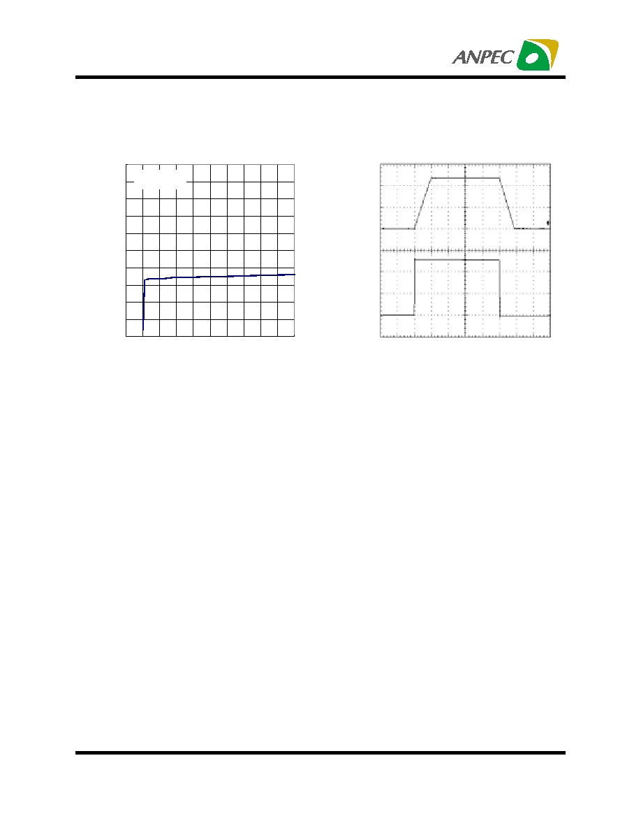
Voltage Follower pulse Response
Time
- µ
s
Input Voltage - V
Output Voltage - V
Figure 9