Äîêóìåíòàöèÿ è îïèñàíèÿ www.docs.chipfind.ru
Copyright
©
ANPEC Electronics Corp.
Rev. A.1 - Jun., 2005
APL5101/2
www.anpec.com.tw
1
ANPEC reserves the right to make changes to improve reliability or manufacturability without notice, and advise
customers to obtain the latest version of relevant information to verify before placing orders.
Features
General Description
The APL5101/2 are micro-power, ultra low dropout
linear regulator, which operate from 2V to 6V input
voltage and deliver up to 150mA. Typical dropout
voltage is only 200mV at 150mA loading. Designed
for use in battery-powered system, the low 4
µ
A
quiescent current makes it an ideal choice. Design
with an internal P-channel MOSFET pass transistor,
the APL5101/2 maintain a low supply current,
independent of the load current and dropout voltage.
Other features include thermal-shutdown protection
and current limit protection to ensure specified
output current and controlled short-circuit current.
The APL5101/2 regulator come in a miniature SOT-23,
SOT-23-5 and SOT-89 packages.
Applications
·
Hand-held Equipment
·
RTC or CMOS Backup Power
·
Battery Powered Equipment
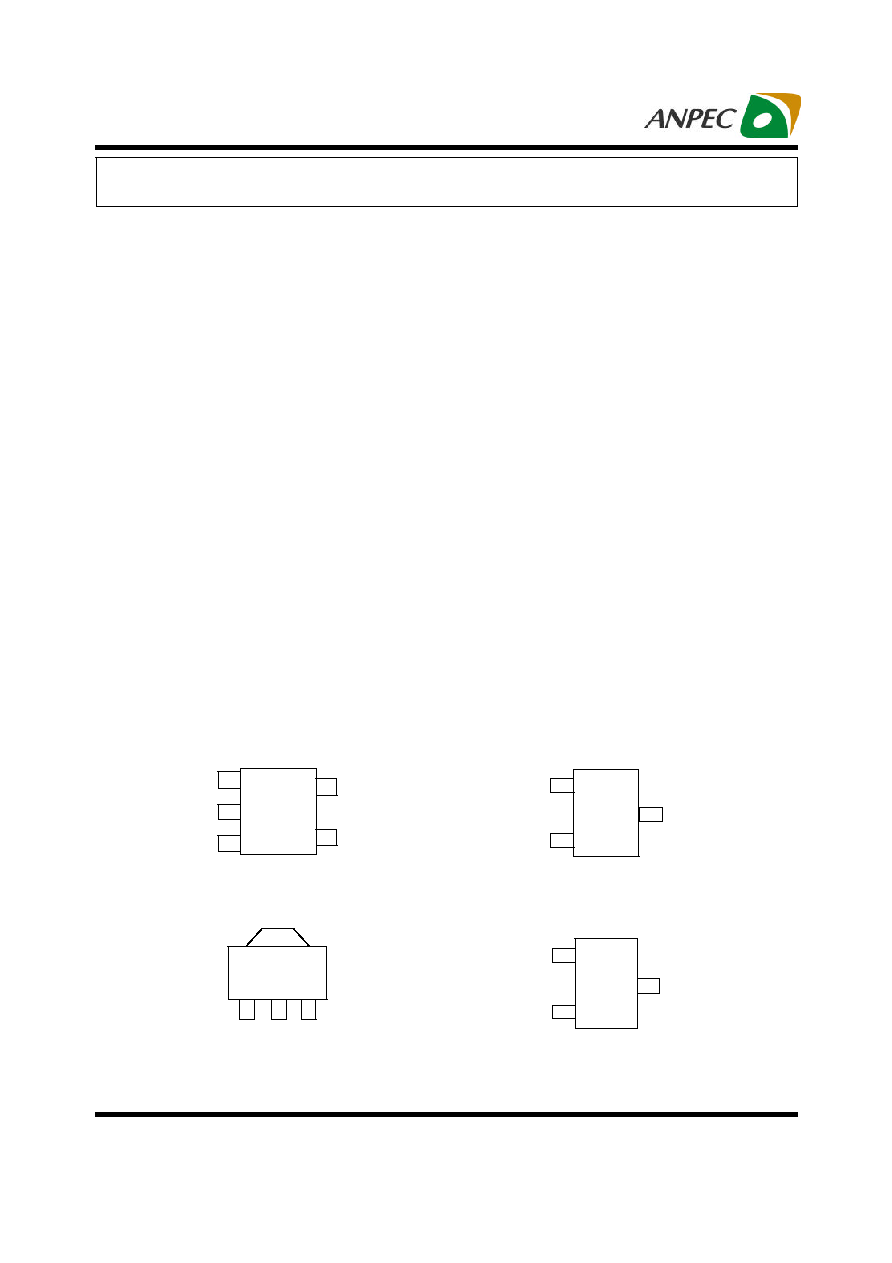
Pin Configuration
SOT-23-5
·
Ultra Low Quiescent Current: 4
µ
A
·
Ultra Low Dropout Voltage:
200mV@3.3V/150mA
·
Fixed Output Voltages: 1.2V~3.5V,
steps 100mV
·
Guaranteed 150mA Output Current
·
Stable with 1
µ
F Output Capacitor
·
Ceramic Capacitor can be used
·
Current Limit Protection
·
Controlled Short Circuit Current: 50mA
·
Build in Thermal Protection
·
SOT-23, SOT-23-5 and SOT-89 packages
·
Lead Free Available (RoHS Compliant)
SOT-23
APL5102
APL5101
SOT-23
APL5101
150mA, 4
µ
A Quiescent Current Regulator
GND
V
OUT
V
IN
APL5101
SOT-89
V
OUT
GND
V
IN
1
2
3
V
OUT
GND
V
IN
1
2
3
1
2
3
V
OUT
GND
V
IN
1
2
3
V
OUT
GND
V
IN
1
2
3
V
IN
GND
SHDN
NC
V
OUT
1
2
3
4
5
V
IN
GND
SHDN
NC
V
OUT
1
2
3
4
5
Copyright
©
ANPEC Electronics Corp.
Rev. A.1 - Jun., 2005
APL5101/2
www.anpec.com.tw
2
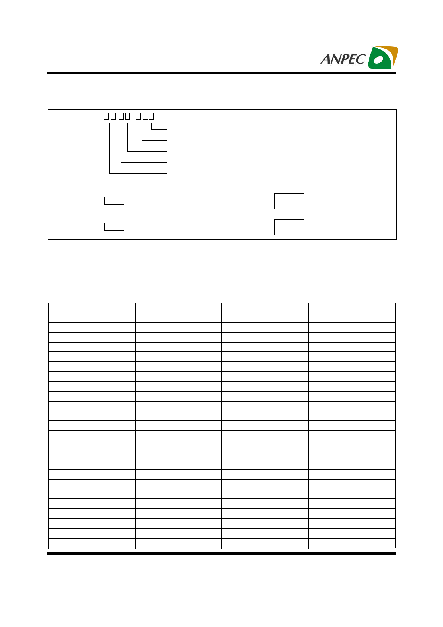
Package Code
A : SOT-23 B : SOT-23-5 D : SOT-89
Operating Ambient Temp. Range
I : -40 to 85 C
Handling Code
TR : Tape & Reel
Voltage Code :
12 : 1.2V ~ 35 : 3.5V
Lead Free Code
L : Lead Free Device Blank : Original Device
APL5101/2 -
Handling Code
Temp. Range
Package Code
Voltage Code
105X
X - Date Code : 5 - 1.2V
APL5101 -12 A/B:
Lead Free Code
APL5101
XXXXX12
XXXXX - Date Code : 12 - 1.2V
APL5101 -12 D :
AB5X
X - Date Code : 5 - 1.2V
APL5102 -12 A/B:
APL5102
XXXXX12
XXXXX - Date Code : 12 - 1.2V
APL5102 -12 D :
Ordering and Marking Information
Product Name
Marking
Product Name
Marking
APL5101-12A/B
105X
APL5102-12A/B
AB5X
APL5101-13A/B
107X
APL5102-13A/B
AB7X
APL5101-14A/B
108X
APL5102-14A/B
AB8X
APL5101-15A/B
109X
APL5102-15A/B
AB9X
APL5101-16A/B
10AX
APL5102-16A/B
ABAX
APL5101-17A/B
10BX
APL5102-17A/B
ABBX
APL5101-18A/B
10CX
APL5102-18A/B
ABCX
APL5101-19A/B
10DX
APL5102-19A/B
ABDX
APL5101-20A/B
10EX
APL5102-20A/B
ABEX
APL5101-21A/B
10FX
APL5102-21A/B
ABFX
APL5101-22A/B
10GX
APL5102-22A/B
ABGX
APL5101-23A/B
10HX
APL5102-23A/B
ABHX
APL5101-24A/B
10IX
APL5102-24A/B
ABIX
APL5101-25A/B
10JX
APL5102-25A/B
ABJX
APL5101-26A/B
10KX
APL5102-26A/B
ABKX
APL5101-27A/B
10LX
APL5102-27A/B
ABLX
APL5101-28A/B
10MX
APL5102-28A/B
ABMX
APL5101-29A/B
10NX
APL5102-29A/B
ABNX
APL5101-30A/B
10OX
APL5102-30A/B
ABOX
APL5101-31A/B
10PX
APL5102-31A/B
ABPX
APL5101-32A/B
10QX
APL5102-32A/B
ABQX
APL5101-33A/B
10RX
APL5102-33A/B
ABRX
APL5101-34A/B
10SX
APL5102-34A/B
ABSX
APL5101-35A/B
10TX
APL5102-35A/B
ABTX
SOT-23 and SOT-23-5 packages
°
Note
:
ANPEC lead-free products contain molding compounds/die attach materials and 100% matte tin plate
termination finish; which are fully compliant with RoHS and compatible with both SnPb and lead-free soldiering
operations. ANPEC lead-free products meet or exceed the lead-free requirements of IPC/JEDEC J STD-020C
for MSL classification at lead-free peak reflow temperature.
Copyright
©
ANPEC Electronics Corp.
Rev. A.1 - Jun., 2005
APL5101/2
www.anpec.com.tw
3
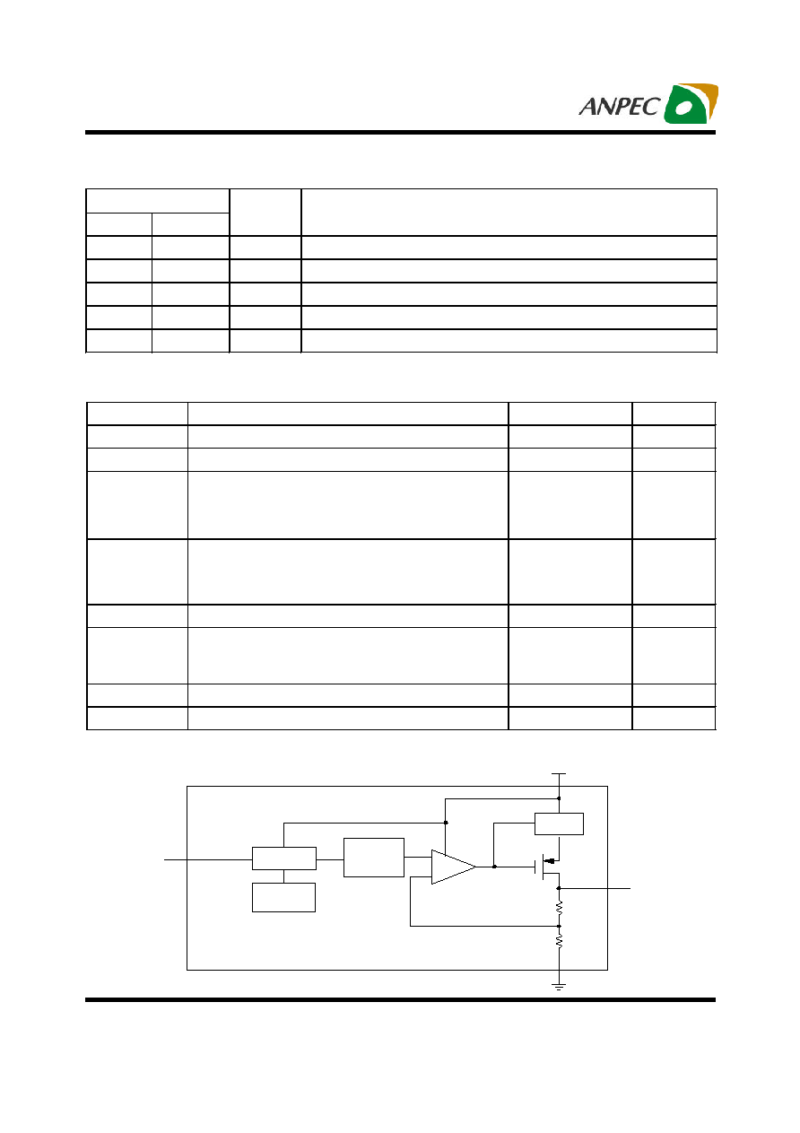
Pin Description
Absolute Maximum Ratings
Symbol
Parameter
Rating
Unit
V
IN
,V
OUT
Input Voltage or Out Voltage
6.5
V
SHDN
V
OUT
Shutdown Control Pin
6.5
V
R
TH,JA
Thermal Resistance-Junction to Ambient
SOT-23
SOT-23-5
SOT-89
260
260
180
°C /W
R
TH,JC
Thermal Resistance-Junction to Ambient
SOT-23
SOT-23-5
SOT-89
130
130
90
°C /W
P
D
Power Dissipation
Internally Limited
W
T
J
Operating Junction Temperature
Control Section
Power Transistor
0 to 125
0 to 140
°C
T
STG
Storage Temperature Range
-65 to +150
°C
T
L
Lead Temperature (Soldering, 10 second)
260
°C
PIN
No.
Name
I/O
Description
1
V
IN
I
Voltage supply input pin
2
GND
GND pin
3
SHDN
I
Shutdown control pin, high = off, low = normal
4
NC
Not connected
5
V
OUT
O
Regulator output pin
Block Diagram
C u r r e n t
L im i t
S h u t d o w n
L o g i c
R e f e r e n c e
V o l t a g e
T h e r m a l
S h u t d o w n
+
_
VIN
V O U T
S H D N
G N D
A P L 5 1 0 1 / 2
Copyright
©
ANPEC Electronics Corp.
Rev. A.1 - Jun., 2005
APL5101/2
www.anpec.com.tw
4
Electrical Characteristics
Unless otherwise noted these specificatons apply over full temperature, V
IN
= 5V, C
IN
= C
OUT
= 1
µ
F,
T
A
= -40 to 85
°
C. Typical values refer to T
A
= 25
°
C.
Note: Dropout voltage definition:V
IN
-V
OUT
when V
OUT
is 2% below the value of V
OUT
for V
IN
= V
OUT
+1V.
APL5101/2
Symbol
Parameter
Test Condition
Min.
Typ.
Max.
Unit
V
IN
Input Voltage
2
6
V
Output Voltage Accuracy
V
IN
= 5V
-2
2
%
V
OUT
Output Voltage Range
1.2
3.5
V
I
LIMIT
Current Limit
V
IN
= 5V
250
300
370
mA
I
OUT
= 0mA
4
7
Quiescent Current
I
OUT
= 150mA
4
10
I
Q
Shutdown Supply Current
V
SHDN
= High
0.1
1
µ
A
I
OUT
Load Current
150
mA
REG
LINE
Line Regulation
V
OUT
+ 0.5V<V
IN
<6V,
I
OUT
= 10mA
2
10
mV
REG
LOAD
Load Regulation
V
IN
= 5V, 0Ma<I
OUT
<I
MAX
15
30
mV
V
OUT
= 1.4V, I
OUT
= 150mA
1000
1300
V
OUT
= 1.8V, I
OUT
= 150mA
600
900
V
DROP
Dropout Voltage
(NOTE)
V
OUT
= 3.3V, I
OUT
= 150mA
200
300
mV
PSRR Ripple Rejection
F = 1kHz, C
OUT
= 1
µ
F,
I
OUT
= 10mA
30
40
dB
I
SHORT
Short Circuit Current
V
OUT
= 0V
40
50
60
mA
e
n
Noise
F = 22Hz to 80kHz,
C
OUT
= 1
µ
F, I
OUT
= 10mA
200
250
µ
V
RMS
I
SHDN
Shutdown Input Bias Current V
SHDN
= Low
0.1
1
µ
A
High Threshold Voltage
1.6
V
IN
+0.3
V
V
SHDN
Low Threshold Voltage
-0.3
0.4
V
T
EXIT
Shutdown Exit Delay
V
OUT
= 90%, R
LOAD
= 25
1.5
2
2.5
mS
Over Temperature Shutdown
120
135
°C
OTS Over Temperature Shutdown
Hysteresis
10
20
30
°C
TC
Output Voltage Temperature
Coefficient
T
A
= -40°C ~ 100°C
100
200
ppm/°C
Output Capacitor
1
10
µ
F
C
OUT
ESR
10
1000
m
Copyright
©
ANPEC Electronics Corp.
Rev. A.1 - Jun., 2005
APL5101/2
www.anpec.com.tw
5
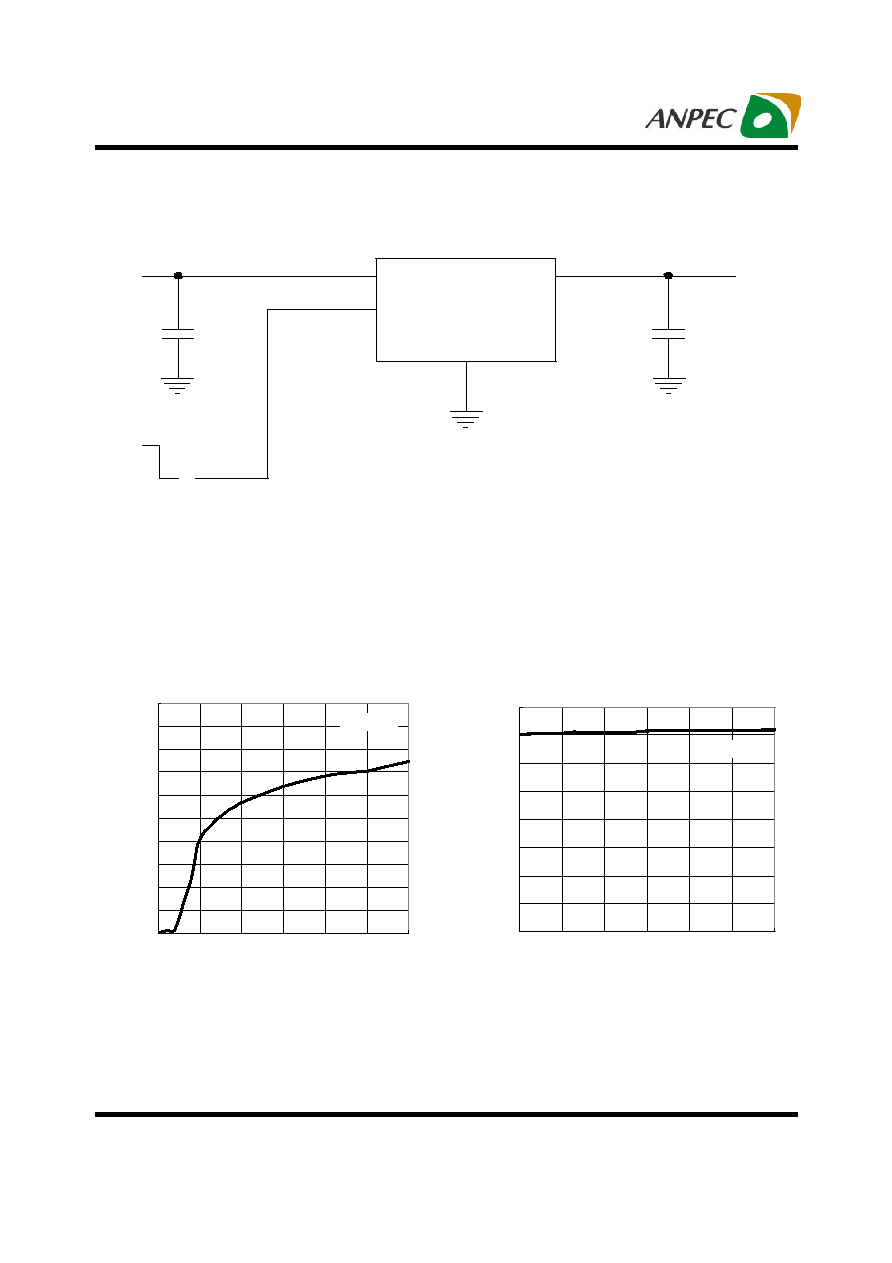
Application Circuit
APL5101/2
V
IN
SHDN
V
OUT
C
OUT
C
IN
GND
1
µ
1
µ
F
F
0
0.5
1
1.5
2
2.5
3
3.5
4
0
25
50
75
100
125
150
0
0.5
1
1.5
2
2.5
3
3.5
4
4.5
5
0
1
2
3
4
5
6
Application Characteristics
V
OUT
=3.3V
Quiescent Current vs. Input Voltage
Input Voltage(V)
Quiescent Current(
µ
A)
V
IN
=5V
Output Current(mA)
Quiescent Current vs. Output Current
Quiescent Current(
µ
A)