Low I
Q
, Low Dropout 150mA Fixed Voltage Regulator
Copyright
©
ANPEC Electronics Corp.
Rev. B.4 - May., 2005
APL5151/2/3/4
www.anpec.com.tw
1
ANPEC reserves the right to make changes to improve reliability or manufacturability without notice, and advise
customers to obtain the latest version of relevant information to verify before placing orders.
Features
General Description
The APL5151/2/3/4 is micropower, low noise, low drop-
out linear regulator. Operate from 3V to 6V input volt-
age and deliver up to 150mA. Typical output noise is
just 60uV
RMS
with the addition of an external 0.33uF
bypass capacitor in BP pin and typical dropout voltage
is only 220mV at 150mA loading. Designed for use in
battery-powered system, the low 50uA quiescent cur-
rent makes it an ideal choice. Design with an internal
P-channel MOSFET pass transistor, the APL5151/2/
3/4 maintains a low supply current, independent of
the load current and dropout voltage. Other features
include reverse current protection, thermal-shutdown
protection, current limit protection to ensure speci-
fied output current and controlled short-circuit current.
The APL5151/2/3/4 regulators come in a miniature SOT-
23-5 package.
Applications
∑
Notebook Computer
∑
PDA or Portable Equipments
∑
Noise-Sensitive Instrumentation Systems
∑
Low Noise : 60uV
RMS
(100Hz to 100kHz)
∑
Low Quiescent Current : 50uA
∑
Low Dropout Voltage : 300mV
(VOUT(Nominal)=3.0V Version @150mA)
∑
Very low Shutdown Current : < 0.5uA
∑
Fixed Output Voltage : 1.3V,1.4V,1.5V,1.6V,
1.7V,1.8V,1.9V, 2.0V,2.1V,2.2V,2.3V,2.4V,
2.5V,2.6V,2.7V, 2.8V, 2.85V,2.9V,3.0V,3.1V,
3.2V,3.3V,3.4V, 3.5V, 5.0V
∑
Stable with 1uF Output Capacitor
∑
Stable with Aluminum , Tantalum or Ceramic
Capacitors
∑
Reverse Current Protection
∑
No Protection Diodes Needed
∑
Built in Thermal Protection
∑
Built in Current Limit Protection
∑
Controlled Short Circuit Current : 50mA
∑
Fast transient Response
∑
Short Setting Time
∑
SOT-23-5 Package
∑
Lead Free Available (RoHS Compliant)
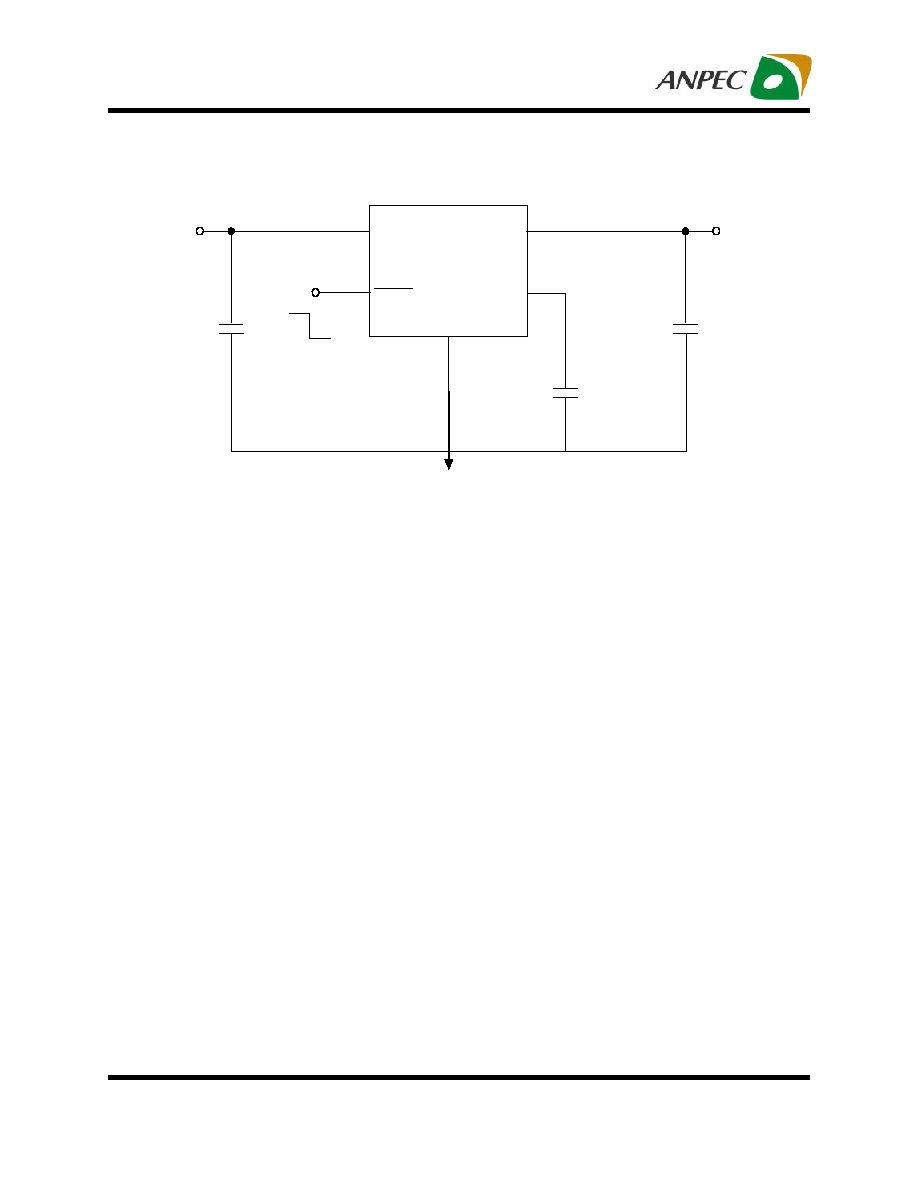
Pin Configuration
V
IN
GND
BP
V
OUT
1
2
3
5
SHDN
4
APL5151
V
IN
GND
BP
V
OUT
1
2
3
5
SHDN
4
APL5152
V
IN
GND
BP
V
OUT
1
2
3
5
SHDN
4
APL5153
V
IN
GND
B P
V
OUT
1
2
3
5
SHDN
4
APL5154

Copyright
©
ANPEC Electronics Corp.
Rev. B.4 - May., 2005
APL5151/2/3/4
www.anpec.com.tw
2
Product
Name
Marking
Product
Name
Marking
Product
Name
Marking
Product
Name
Marking
APL5151-13
1517X
APL5152-13
1527X
APL5153-13
1537X
APL5154-13
1547X
APL5151-14
1518X
APL5152-14
1528X
APL5153-14
1538X
APL5154-14
1548X
APL5151-15
1519X
APL5152-15
1529X
APL5153-15
1539X
APL5154-15
1549X
APL5151-16
151AX
APL5152-16
152AX
APL5153-16
153AX
APL5154-16
154AX
APL5151-17
151BX
APL5152-17
152BX
APL5153-17
153BX
APL5154-17
154BX
APL5151-18
151CX
APL5152-18
152CX
APL5153-18
153CX
APL5154-18
154CX
APL5151-19
151DX
APL5152-19
152DX
APL5153-19
153DX
APL5154-19
154DX
APL5151-20
151EX
APL5152-20
152EX
APL5153-20
153EX
APL5154-20
154EX
APL5151-21
151FX
APL5152-21
152FX
APL5153-21
153FX
APL5154-21
154FX
APL5151-22
151GX
APL5152-22
152GX
APL5153-22
153GX
APL5154-22
154GX
APL5151-23
151HX
APL5152-23
152HX
APL5153-23
153HX
APL5154-23
154HX
APL5151-24
151IX
APL5152-24
152IX
APL5153-24
153IX
APL5154-24
154IX
APL5151-25
151JX
APL5152-25
152JX
APL5153-25
153JX
APL5154-25
154JX
APL5151-26
151KX
APL5152-26
152KX
APL5153-26
153KX
APL5154-26
154KX
APL5151-27
151LX
APL5152-27
152LX
APL5153-27
153LX
APL5154-27
154LX
APL5151-28
151MX
APL5152-28
152MX
APL5153-28
153MX
APL5154-28
154MX
APL5151-285
1512X
APL5152-285
1522X
APL5153-285
1532X
APL5154-285
1542X
APL5151-29
151NX
APL5152-29
152NX
APL5153-29
153NX
APL5154-29
154NX
APL5151-30
151OX
APL5152-30
152OX
APL5153-30
153OX
APL5154-30
154OX
APL5151-31
151PX
APL5152-31
152PX
APL5153-31
153PX
APL5154-31
154PX
APL5151-32
151QX
APL5152-32
152QX
APL5153-32
153QX
APL5154-32
154QX
APL5151-33
151RX
APL5152-33
152RX
APL5153-33
153RX
APL5154-33
154RX
APL5151-34
151SX
APL5152-34
152SX
APL5153-34
153SX
APL5154-34
154SX
APL5151-35
151TX
APL5152-35
152TX
APL5153-35
153TX
APL5154-35
154TX
APL5151-48
151XX
APL5152-48
152XX
APL5153-48
153XX
APL5154-48
154XX
APL5151-49
151YX
APL5152-49
152YX
APL5153-49
153YX
APL5154-49
154YX
APL5151-50
151ZX
APL5152-50
152ZX
APL5153-50
153ZX
APL5154-50
154ZX
Ordering Information
Package Code
B : SOT-23-5
Temp. Range
C : 0 to 70 C I : -40 to 85 C
Handling Code
TR : Tape & Reel
Voltage Code :
13 : 1.3V ~ 50 : 5.0V(refer below for detailed)
Lead Free Code
L : Lead Free Device Blank : Original Device
APL5151/2/3/4 -
Handling Code
Temp. Range
Package Code
Voltage Code
Lead Free Code
∞
∞
Marking Information
The last character "X" in the marking is for data code.
Note: ANPEC lead-free products contain molding compounds/die attach materials and 100% matte in plate termina-
tion finish; which are fully compliant with RoHS and compatible with both SnPb and lead-free soldiering operations.
ANPEC lead-free products meet or exceed the lead-free requirements of IPC/JEDEC J STD-020C for MSL classifica-
tion at lead-free peak reflow temperature.
Copyright
©
ANPEC Electronics Corp.
Rev. B.4 - May., 2005
APL5151/2/3/4
www.anpec.com.tw
3
PIN
No.
Name
I/O
Description
1
V
IN
I
Supply voltage input.
2
GND
Ground pins of the circuitry, and all ground pins must be soldered to
PCB with proper power dissipation.
3
SHDN
I
Shutdown control pin, low = off , high = normal .
4
BP
O
Bypass signal pin in fixed output type device
5
V
OUT
O
Output pin of the regulator.
Pin Description
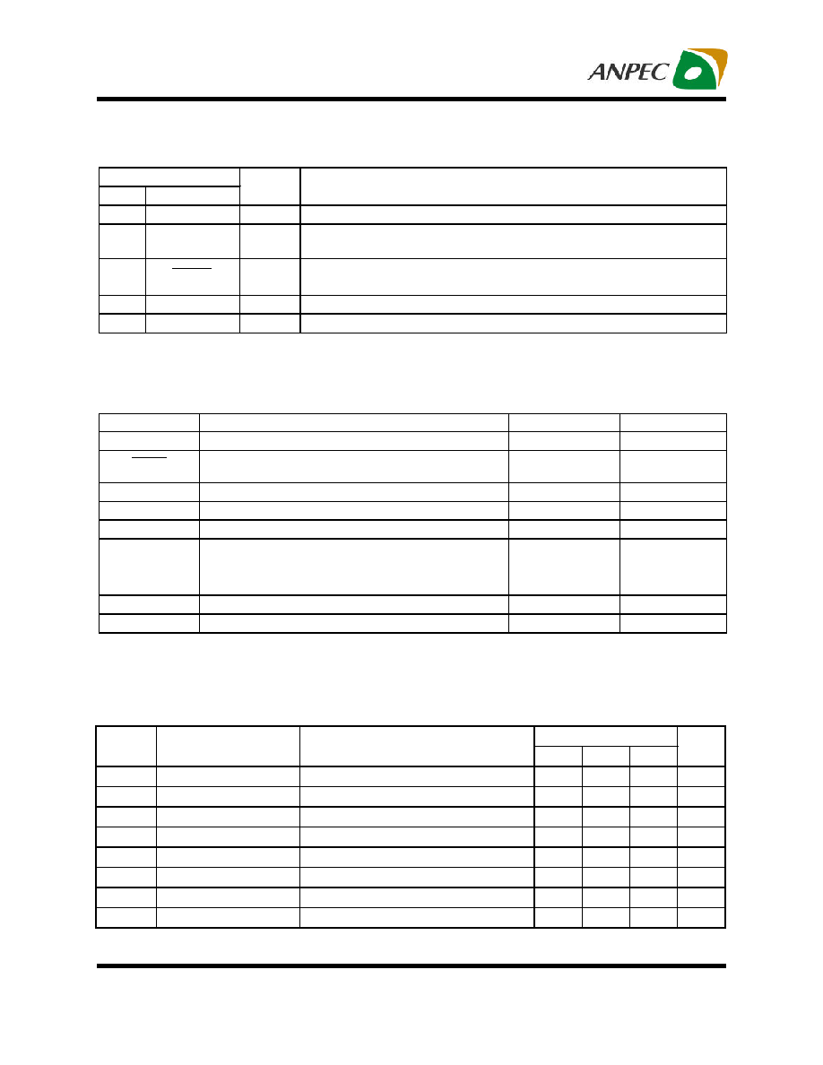
Absolute Maximum Ratings
Symbol
Parameter
Rating
Unit
V
IN
, V
OUT
Input Voltage or Out Voltage
6
V
SHDN
Shutdown Control Pin
6
V
R
TH,JA
Thermal Resistance ≠ Junction to Ambient
260
∞
C/W
R
TH,JC
Thermal Resistance ≠ Junction to Case
130
∞
C/W
P
D
Power Dissipation
Internally Limited
W
T
J
Operating Junction Temperature
∞
C
Control Section
0 to 125
Power Transistor
0 to 150
T
STG
Storage Temperature Range
-65 to +150
∞
C
T
L
Lead Temperature (Soldering, 10 second)
260
∞
C
Electrical Characteristics
Unless otherwise noted these specifications apply over full temperature , V
IN
=3.6V, C
IN
=C
OUT
=1uF, SHDN=V
IN
,
T
J
=0 to 125
∞
C . Typical values refer to T
J
=25
∞
C .
APL5151/2/3/4
Symbol
Parameter
Test Conditions
Min.
Typ.
Max.
Unit
V
IN
Input Voltage
2.7
6
V
V
OUT
Output Voltage
V
OUT
+1.0V< V
CC
<6.0V, 0mA< I
OUT
< I
MAX
V
OUT
-2
%
V
OUT
V
OUT
+2
%
V
I
LIMIT
Circuit Current Limit
V
IN
=V
OUT
+1V
250
300
350
mA
I
SHORT
Short Current
V
OUT
=0V
40
50
60
mA
I
OUT
Load Current
150
mA
REG
LINE
Line Regulation
V
OUT
+0.5V< V
CC
<6.0V, 0mA< I
OUT
< I
MAX
4
10
mV
REG
LOAD
Load Regulation
V
IN
=V
OUT
+1.0V, 0mA< I
OUT
< I
MAX
515X
1
0.1
6
mV
%
Load Transient
V
IN
= V
OUT
+1V , I
OUT
=1mA-150mA in 1
µ
s
10? A to max. load in 1? s
70
150
mV
mV

Copyright
©
ANPEC Electronics Corp.
Rev. B.4 - May., 2005
APL5151/2/3/4
www.anpec.com.tw
4
Electrical Characteristics (Cont.)
Unless otherwise noted these specifications apply over full temperature , V
IN
=3.6V, C
IN
=C
OUT
=1uF, SHDN=V
IN
,
T
J
=0 to 125
∞
C . Typical values refer to T
J
=25
∞
C .
APL5151/2/3/4
Symbol
Parameter
Test Conditions
Min.
Typ.
Max.
Unit
PSRR Ripple Rejection
F
1kHz, 1Vpp at V
IN
= V
OUT
+1.0V
C
BP
=0.1
µ
F, C
OUT
= 1
µ
F
45
55
dB
1.3V
V
OUT
<1.5V
1.2
1.4
1.5V
V
OUT
<2.0
1
1.2
2.0V
V
OUT
<2.5
0.7
0.8
2.5V
V
OUT
<3
0.3
0.4
V
DROP
Dropout Voltage
(Note)
I
OUT
=150mA
3V
V
OUT
5
0.2
0.3
V
No load
50
80
I
Q
Quiescent Current
I
OUT
=150mA
135
170
µ
A
Shutdown Supply
Current
Shutdown = low
I
OUT
=0, V
CC
=6.0V
0.01
1
µ
A
100Hz<f<100kHz, typical load,
C
BP
=0.1
µ
F, C
OUT
= 1
µ
F
80
Noise
100Hz<f<100kHz, typical load,
C
BP
=0.33
µ
F, C
OUT
= 1
µ
F
60
µ
Vrms
C
BP
=0.1
µ
F,C
OUT
=1
µ
F, no load
4
Shutdown Recovery
Delay
C
BP
=0.33
µ
F,C
OUT
=1
µ
F, no load
13.2
ms
OTS
Over Temperature
Shutdown
150
∞
C
Over Temperature
Shutdown Hysteresis
Hysteresis
10
∞
C
TC
Output Voltage
Temperature
Coefficient
50
ppm/
∞
C
C
OUT
Output Capacitor
0.8
1.0
2.6
µ
F
ESR
0.02
0.1
1
Ohm
Shutdown Input
Threshold
V
OUT
+1.0V< V
IN
<6.0V
0.4
1.6
2.5
V
I
SHDN
Shutdown Input Bias
Current
V
SHDN
=V
IN
0.01
100
nA
Input Reverse Leakage
Current
V
OUT
-V
IN
=0.1V
0.1
0.5
µ
A
Reverse Protection
Threshold
11
50
mV
Note: Dropout voltage definition : V
IN
-V
OUT
when V
OUT
is 2% below the value of V
OUT
for V
IN
= V
OUT
+ 0.5V