Low I
Q
, Low Dropout 300mA Fixed Voltage Regulator
Copyright
ANPEC Electronics Corp.
Rev. B.1 - Mar., 2004
APL5301/2
www.anpec.com.tw
1
ANPEC reserves the right to make changes to improve reliability or manufacturability without notice, and advise
customers to obtain the latest version of relevant information to verify before placing orders.
Features
The APL5301/2 series are micropower, low noise, low
dropout linear regulators, which operate from 3V to
6V input voltage and deliver up to 300mA. Typical
dropout voltage is only 260mV at 300mA loading. De-
signed for use in battery-powered system, the low 50uA
quiescent current makes it an ideal choice. Design
with an internal P-channel MOSFET pass transistor,
the APL5301/2 maintain a low supply current, inde-
pendent of the load current and dropout voltage.
Other features include reverse current protection, ther-
mal-shutdown protection, current limit protection to
ensure specified output current and controlled short-
circuit current. The APL5301/2 regulators come in a
miniature SOP-8, SOT-23, SOT-23-5, SOT-89 and
SOT-89-5 packages.
Applications
∑
Notebook Computer
∑
PDA or Portable Equipments
∑
Noise-Sensitive Instrumentation Systems
∑∑
∑∑
∑
Low Quiescent Current : 50uA (No load)
∑∑
∑∑
∑
Low Dropout Voltage : 400mV
(VOUT(Nominal)=3.0V Version @300mA)
∑∑
∑∑
∑
Very low Shutdown Current : < 0.5uA
∑∑
∑∑
∑
Fixed Output Voltage : 1.3V ~ 5.0V
by step 0.1V increment
∑∑
∑∑
∑
Stable with 1uF Output Capacitor
∑∑
∑∑
∑
Stable with Aluminum, Tantalum or Ceramic
Capacitors .
∑∑
∑∑
∑
Reverse Current Protection
∑∑
∑∑
∑
No Protection Diodes Needed
∑∑
∑∑
∑
Built in Thermal Protection
∑∑
∑∑
∑
Built in Current Limit Protection
∑∑
∑∑
∑
Controlled Short Circuit Current : 50mA
∑∑
∑∑
∑
Fast Transient Response
∑∑
∑∑
∑
Short Setting Time
∑∑
∑∑
∑
SOP-8, SOT-23, SOT-23-5, SOT-89,
and SOT-89-5 Packages
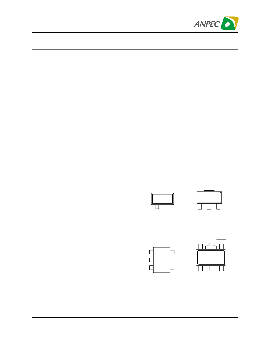
Pin Configuration
APL5301
SOT-89 (Top View)
G N D
V
IN
V
O U T
1
2
3
T A B is V
IN
SOT-23 (Top
View)
G N D
1
2
3
V
O U T
V
IN
APL5301
V
IN
G N D
B P
V
O U T
1
2
3
5
S H D N
4
APL5301
SOT-23-5 (Top
View)
APL5301
SOT-89-5 (Top
View)
V
IN
G N D
V
O U T
1
2
3
5
4
S H D N
B P
G N D
General Description

Copyright
ANPEC Electronics Corp.
Rev. B.1 - Mar., 2004
APL5301/2
www.anpec.com.tw
2
P a c k a g e C o d e
A : S O T -2 3 B : S O T -2 3 -5 D : S O T -8 9
D 5 : S O T -8 9 -5 K : S O P -8
T e m p . R a n g e
C : 0 to 7 0 C I : -4 0 to 8 5 C
H a n d lin g C o d e
T R : T a p e & R e e l
V o lta g e C o d e :
1 3 : 1 .3 V ~ 3 4 : 3 .4 V 5 0 : 5 .0 V
L e a d F re e C o d e
L : L e a d F re e D e v ic e B la n k : O rig in a l D e v ic e
A P L 5 3 0 1 /2 -
H a n d lin g C o d e
T e m p . R a n g e
P a c k a g e C o d e
V o lta g e C o d e
A P L 5 3 0 1 /2
X X X X X 1 3
X X X X X - D a te C o d e ; 1 3 - 1 .3 V
A P L 5 3 0 1 /2 -1 3 D /K :
L e a d F re e C o d e
Product Name
Marking
Product Name
Marking
APL5301-13A/B
317X
APL5302-13A/B
327X
APL5301-14A/B
318X
APL5302-14A/B
328X
APL5301-15A/B
319X
APL5302-15A/B
329X
APL5301-16A/B
31AX
APL5302-16A/B
32AX
APL5301-17A/B
31BX
APL5302-17A/B
32BX
APL5301-18A/B
31CX
APL5302-18A/B
32CX
APL5301-19A/B
31DX
APL5302-19A/B
32DX
APL5301-20A/B
31EX
APL5302-20A/B
32EX
APL5301-21A/B
31FX
APL5302-21A/B
32FX
APL5301-22A/B
31GX
APL5302-22A/B
32GX
APL5301-23A/B
31HX
APL5302-23A/B
32HX
APL5301-24A/B
31IX
APL5302-24A/B
32IX
APL5301-25A/B
31JX
APL5302-25A/B
32JX
APL5301-26A/B
31KX
APL5302-26A/B
32KX
APL5301-27A/B
31LX
APL5302-27A/B
32LX
APL5301-28A/B
31MX
APL5302-28A/B
32MX
APL5301-29A/B
31NX
APL5302-29A/B
32NX
APL5301-30A/B
31OX
APL5302-30A/B
32OX
APL5301-31A/B
31PX
APL5302-31A/B
32PX
Marking Information
SOT-23 and SOT-23-5 packages
V
IN
G N D
B P
V
O U T
1
2
3
5
S H D N
4
Pin Configuration (Cont.)
APL5302
SOT-89 (Top View)
SOT-23 (Top
View)
APL5302
Ordering and Marking Information
∞
∞
SOP-8 (Top View)
1
2
3
4
5
6
7
8
S H D N
V
IN
V
O U T
B P
G N D
G N D
G N D
G N D
APL5301
G N D
V
IN
V
O U T
1
2
3
T A B is G N D
G N D
1
2
3
V
O U T
V
IN
SOT-23-5 (Top
View)
APL5302

Copyright
ANPEC Electronics Corp.
Rev. B.1 - Mar., 2004
APL5301/2
www.anpec.com.tw
3
Product Name
Marking
Product Name
Marking
APL5301-32A/B 31QX APL5302-32A/B 32QX
APL5301-33A/B 31RX APL5302-33A/B 32RX
APL5301-34A/B 31SX APL5302-34A/B 32SX
APL5301-35A/B 31TX APL5302-35A/B 32TX
APL5301-48A/B 31XX APL5302-48A/B 32XX
APL5301-49A/B 31YX APL5302-49A/B 32YX
APL5301-50A/B 31ZX APL5302-50A/B 32ZX
Pin Description
PIN
No.
Name
I/O
Description
1
V
IN
I
Supply voltage input.
2
GND
Ground pins of the circuitry, and all ground pins must be soldered
To PCB with proper power dissipation.
3
SHDN
(Note1)
I
Shutdown control pin, low = off, high = nromal.
4
BP
(Note1)
O
Bypass signal pin of the regulator.
5
V
OUT
O
Output pin of the regulator.
Note1 : This pin does not exist in 3-pin package.
Marking Information (Cont.)
SOT-23 and SOT-23-5 packages
Symbol Parameter Rating
Unit
V
IN
, V
OUT
Input Voltage or Out Voltage
6.5
V
SHDN
Shutdown Control Pin
6.5 V
R
TH,JA
Thermal Resistance ≠ Junction to Ambient
357
∞C/W
P
D
Power Dissipation
Internally Limited
W
T
J
Operating Junction Temperature
∞C
Control Section
0 to 125
Power Transistor
0 to 150
T
STG
Storage Temperature Range
-65 to +150
∞C
T
L
Lead Temperature (Soldering, 10 second)
260 ∞C
Absolute Maximum Ratings
The last character "X" in the marking is for data code.
Don't leave open.
Copyright
ANPEC Electronics Corp.
Rev. B.1 - Mar., 2004
APL5301/2
www.anpec.com.tw
4
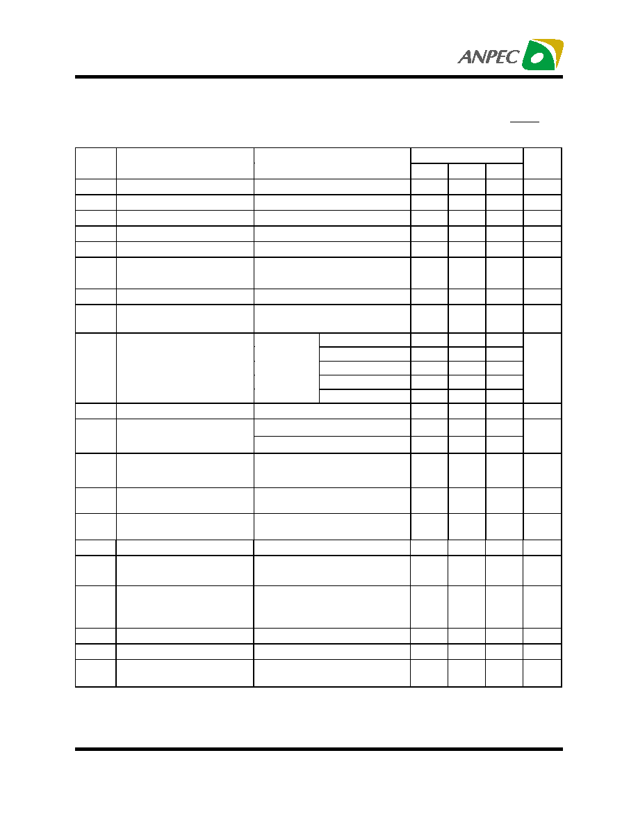
Electrical Characteristics
Unless otherwise noted these specifications apply over full temperature, V
IN
=3.8V, C
IN
=C
OUT
=1uF, SHDN=V
IN
,
T
J
=0 to 125
∞
C. Typical values refer to T
J
=25
∞
C.
APL5301/2
Symbol Parameter
Test
Conditions
Min. Typ. Max.
Unit
V
IN
Input
Voltage
2.7
6.5
V
V
OUT
Output
Voltage
V
OUT
+1.0V< V
CC
<6.0V, 0mA< I
OUT
V
OUT
-2
%
V
OUT
V
OUT
+2
%
V
I
LIMIT
Circuit Current Limit
V
IN
=V
OUT
+0.5V
500 mA
I
SHORT
Short
Current
V
OUT
=0V
50 mA
I
OUT
Load Current
V
IN
=V
OUT
+0.5V
300
mA
REG
LINE
Line Regulation
V
OUT
+0.5V< V
CC
<6.0V,
I
OUT
=150mA
4
10
mV
REG
LOA
Load Regulation
V
IN
=V
OUT
+0.5V, 0mA< I
OUT
< I
MAX
1
6
mV
Load
Transient
V
IN
= V
OUT
+0.5V ,
I
OUT
=1mA-150mA in 1us
70
150
mV
mV
1.3V
V
OUT
<1.5V 1.2
1.6
1.5V
V
OUT
<2.0V 1
1.2
2.0V
V
OUT
<2.5V 0.8
0.9
2.5V
V
OUT
<3V
0.6
0.7
V
DROP
Dropout
Voltage
(Note2)
I
OUT
=300mA
3V
V
OUT
5V
0.4
0.5
V
PSRR Ripple Rejection
F
1kHz, 1Vpp at V
IN
= V
OUT
+1.0V
45 55 dB
No load
50 80
I
Q
Quiescent Current
I
OUT
=300mA
150 180
µ
A
Shutdown Supply
Current
(Note3)
Shutdown = low
I
OUT
=0, V
CC
=6.0V
0.01
1
µ
A
Noise
100Hz<f<100kHz, typical load,
C
BP
=0.01uF, C
OUT
= 1uF
200
µ
Vrms
Shutdown Recovery
Delay
(Note3)
C
BP
=0.01uF,C
OUT
=1uF, no load
0.4 ms
OTS Over Temperature Shutdown
150
∞
C
Over Temperature Shutdown
Hysteresis
Hysteries
10
∞
C
TC
Output Voltage Temperature
Coefficient
50
ppm/
∞
C
C
OUT
Output Capacitor
0.8 1.0 2.6
µ
F
ESR
0.02
0.1
1
Ohm
Shutdown Input
Threshold
(Note3)
V
OUT
+1.0V< V
IN
<6.0V
0.4 1.6 2.5 V
Copyright
ANPEC Electronics Corp.
Rev. B.1 - Mar., 2004
APL5301/2
www.anpec.com.tw
5
APL5301/2
Symbol
Parameter
Test Conditions
Min.
Typ.
Max.
Unit
I
SHDN
Shutdown input Bias
current
(Note3)
V
SHDN
=V
IN
0.01
100
nA
Input Reverse Leakage
current
V
OUT
-V
IN
=0.1V
0.1
0.5
µ
A
Reverse Protection
Threshold
11
50
mV
Electrical Characteristics (Cont.)
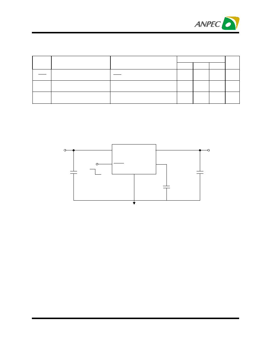
Application Circuit
B P
V
O U T
V
IN
G N D
S H D N
V O U T
C
IN
1 u F
o ff
o n
A P L 5 3 0 1 /2
IN P U T
2 .7 V to 6 V
0 .0 1 u F
C
B P
C
O U T
1 u F
Note2 : Dropout voltage definition : V
IN
-V
OUT
when V
OUT
is 2% below the value of V
OUT
for V
IN
= V
OUT
+ 0.5V
Note3 : For 5-pin devices only.
Copyright
ANPEC Electronics Corp.
Rev. B.1 - Mar., 2004
APL5301/2
www.anpec.com.tw
6
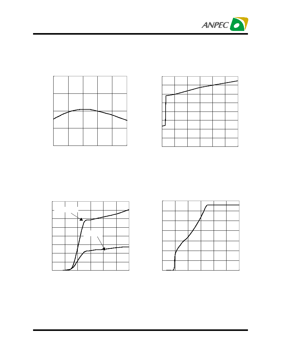
Typical Characteristics
(All Curves are For Fix 3.3V)
0
20
40
60
80
100
120
140
160
0
1
2
3
4
5
6
Ground Pin Current vs. Input Voltage
Input Voltage (V)
Ground Pin Current vs. Load Current (uA)
I
OUT
=50mA
NO LOAD
0
0.5
1
1.5
2
2.5
3
3.5
0
1
2
3
4
5
6
Input Voltage vs. Output Voltage
Input Voltage (V)
Output V
oltage (V)
0
20
40
60
80
100
120
140
160
0
50
100
150
200
250
300
Ground Pin Current vs. Load Current
Ground Pin Current vs. Load Current (uA)
Load Current (mA)
3.28
3.29
3.3
3.31
3.32
-40
-15
10
35
60
85
Output Voltage vs. Temperature
Temperature (∞C )
Output V
oltage (V)
Copyright
ANPEC Electronics Corp.
Rev. B.1 - Mar., 2004
APL5301/2
www.anpec.com.tw
7
0
50
100
150
200
250
300
0
50
100
150
200
250
300
Typical Characteristics
1
1.1
1.2
1.3
1.4
1.5
1.6
3.5
4
4.5
5
5.5
6
SHDN Threshold Voltage vs. Input Voltage
SHDN Threshold V
oltage (V)
Input Voltage (V)
-80
+0
-70
-60
-50
-40
-30
-20
-10
10
200k
20
50
100 200
500
1k
2k
5k
10k 20k
50k
PSRR vs. Frequency
Frequency (H
Z
)
PSRR (dB)
V
IN
=4.3V
I
OUT
=50mA
C
OUT
=1uF
C
BP
=0.1uF
0
0.1
0.2
0.3
0.4
0.5
0.6
0.7
0.8
0.9
1
0
1
2
3
4
5
6
Reverse Leakage Current vs. Output Voltage
Reverse Leakage Current (uA)
Output Voltage (V)
Dropout Voltage vs. Load Current
Load Current (mA)
Dropout V
oltage (mV)

Copyright
ANPEC Electronics Corp.
Rev. B.1 - Mar., 2004
APL5301/2
www.anpec.com.tw
8
Typical Characteristics
1mA
50mA
Load-Transient Response
Output V
oltage (20mV/div)
V
OUT
I
OUT
4V
5V
Time (500us/div)
V
OUT
V
IN
I
OUT
=50mA
Line-Transient Response
V
IN
=4.3V
Output V
oltage (50mV/div)
Time (100us)
2.5V
0V
0V
Time (0.1ms/div)
Entering Shutdown
V
OUT
SHDN
Shutdown Exit Delay
Time (0.1ms/div)
SHDN
C
BP
=0.01uF
V
OUT
Copyright
ANPEC Electronics Corp.
Rev. B.1 - Mar., 2004
APL5301/2
www.anpec.com.tw
9
0.01
0.1
1
10
0
50
100
150
200
250
300
Typical Characteristics
Region of Stable ESR vs. Load Current
Load Current (mA)
C
OUT
ESR (
)
Stable
Region
Untested
C
OUT
=1uF
Recommended Minimum Footprint

Copyright
ANPEC Electronics Corp.
Rev. B.1 - Mar., 2004
APL5301/2
www.anpec.com.tw
10
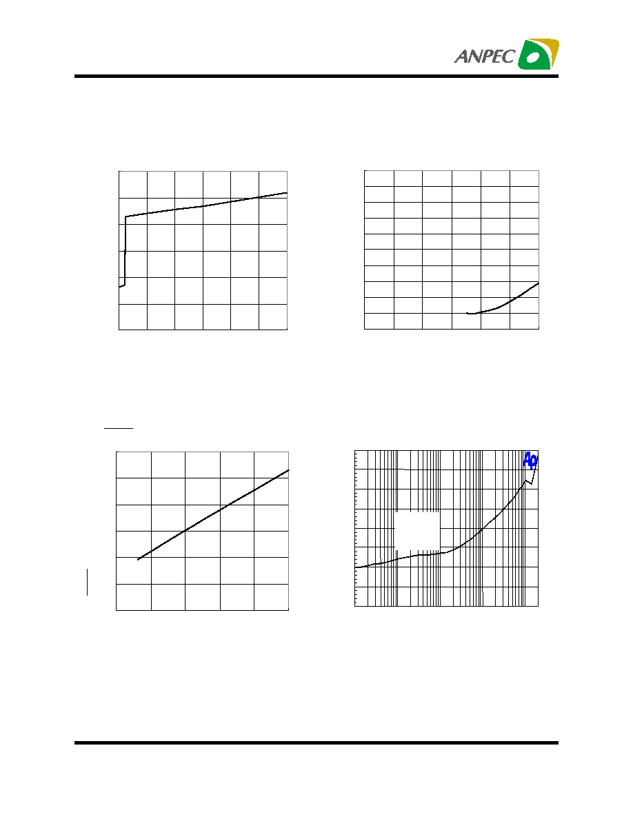
tery-powered systems, this will determine the useful
end-of-life battery voltage. Because the APL5301/2
use a p-channel MOSFET pass transistor, the drop-
out voltage is a function of drain-to-source on-resis-
tance (R
DS(ON)
) multiplied by the load current.
The APL5301/2 load-transient response graphs in typi-
cal characteristics show the transient response. A
step change in the load current from 1mA to 50mA at
1us will cause a 60mV transient spike. Larger output
capacitor and lower ESR can reduce transient spike.
Application Information
Capacitor Selection and Regulator
Stability
The APL5301/2 use at least a 1uF capacitor on the
input, and this capacitor can be Aluminum, Tantalum
or Ceramic capacitor. The input capacitor with larger
value and lower ESR provides better PSRR and line-
transient response. The output capacitor also can use
Aluminum, Tantalum or Ceramic capacitor, and a mini-
mum value of 1uF and ESR above 0.06
is
recommended. The curve of the stable region in typi-
cal characteristics shows the appropriate output ca-
pacitor ESR for different load current stable operation.
A larger output capacitor can reduce noise and im-
prove load-transient response, stability, and PSRR.
Note that some ceramic dielectrics exhibit large ca-
pacitance and ESR variation with temperature. When
using this capacitor, a minimum 2.2uF or more may
be required to ensure the stability at low temperature
operation. Use a bypass capacitor at BP pin for low
output noise. Increasing the capacitance will slightly
decrease the output noise, but increase the start-up
time. (See Shutdown Exit Delay and Output Noise
v s . B y p a s s C a p a c i t o r g r a p h i n t h e t y p i c a l
characteristics)
Load-Transient Considerations
Reverse Current Protection
The APL5301/2 have an internal reverse protection, it
does not need an external schottky diode to connect
the regulator input and output. If the output voltage is
forced above the input voltage by more than 11mV,
the IC will be shutdown and the ground pin current is
below 0.1uA.
Current Limit
The APL5301/2 have a current limit protection. The
ouptut voltage will drop close to zero volt, when load
current reaches the limit, and then the load current
will be limited at 50mA after output voltage is below 0.
7V. When the load current back to the value where
limiting started, the output voltage and current will re-
turn to normal value. When output is shorted to
ground, the APL5301/2 will keep short circuit current
at 150mA .
Input-Output (Dropout)Voltage
The minimum input-output voltage difference (dropout)
Shutdown/Enable
The APL5301/2 have an active high enable function.
Force EN high (>1.6V) enables the regulator, EN low
(<0.4V) disables the regulator and enter the shutdown
mode. In shutdown mode, the quiescent current can
reduce below 1uA. The EN pin cannot be floating, a
floating EN pin may cause an indeterminate state on
the output. If it is no use, connect to V
IN
for normal
operation.
determines the lowest usable supply voltage. In bat

Copyright
ANPEC Electronics Corp.
Rev. B.1 - Mar., 2004
APL5301/2
www.anpec.com.tw
11
Thermal protection limits total power dissipation in the
device. When the junction temperature exceeds
T
J
=+150
∞
C, the thermal sensor generates a logic sig-
nal to turn off the pass transistor and allows IC to
cool. When the IC's junction temperature is down by
10
∞
C, the thermal sensor will turn the pass transistor
on again, resulting in a pulsed output during continu-
ous thermal protection. Thermal protection is designed
to protect the APL5301/2 in the event of fault
conditions. For continuous operation, do not exceed
the absolute maximum junction temperature of
T
J
=+150
∞
C.
Operating Region and Power Dis-
sipation
The thermal resistance of the case to circuit board,
and the rate of air flow all control the APL5301/2's
maximum power dissipation. The power dissipation
across the device is P
D
= I
OUT
(V
IN
-V
OUT
) and the maxi-
mum power dissipation is:
P
DMAX
= (T
J
-T
A
) / (
JC
+
CA
)
where T
J
-T
A
is the temperature difference between the
junction and ambient air,
JC
is the thermal resistance
of the package, and
CA
is the thermal resistance
through the printed circuit board, copper traces, and
other materials to the ambient air.
The GND pin of the APL5301 and APL5302 that the
packages ard SOT-23-5, SOT-89-5 AND SOP-8 pro-
vide an electrical connection to ground and channel-
ing heat away. If power dissipation is large, connect
the GND pin to ground using a large pad or ground
plane, can improve the problem of over heat of IC.
Thermal Protection

Copyright
ANPEC Electronics Corp.
Rev. B.1 - Mar., 2004
APL5301/2
www.anpec.com.tw
12
M i ll i m e t er s
I n c h e s
D i m
M i n .
M a x .
M i n .
M a x .
A
1 . 3 5
1 . 7 5
0 . 0 5 3
0 . 0 6 9
A 1
0 . 1 0
0 . 2 5
0 . 0 0 4
0 . 0 1 0
D
4 . 8 0
5 . 0 0
0 . 1 8 9
0 . 1 9 7
E
3 . 8 0
4 . 0 0
0 . 1 5 0
0 . 1 5 7
H
5 . 8 0
6 . 2 0
0 . 2 2 8
0 . 2 4 4
L
0 . 4 0
1 . 2 7
0 . 0 1 6
0 . 0 5 0
e 1
0 . 3 3
0 . 5 1
0 . 0 1 3
0 . 0 2 0
e 2
1 . 2 7 B S C
0 . 5 0 B S C
1
8
∞
8
∞
H
E
e 1
e 2
0.015X45
D
A
A 1
0 . 0 0 4 m a x .
1
L
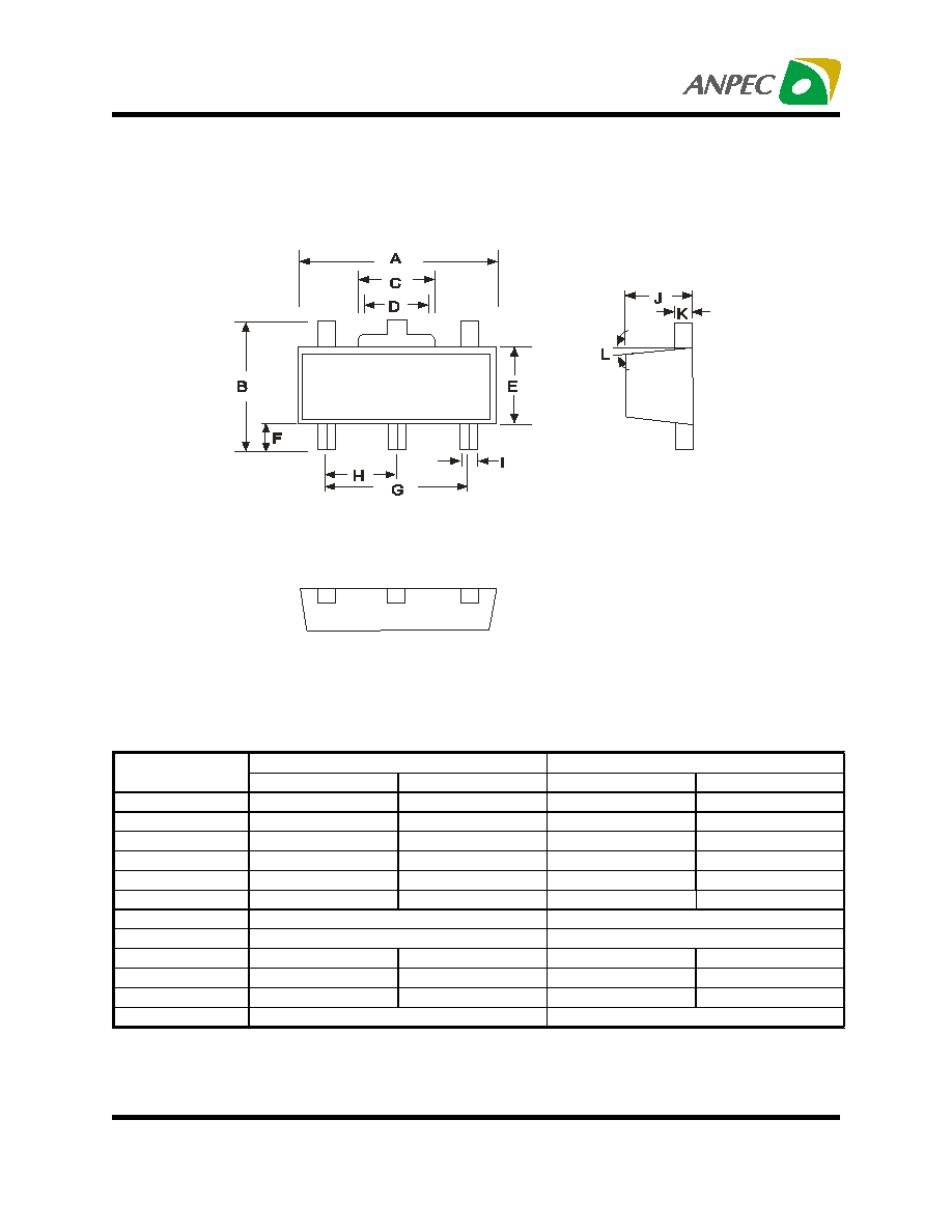
SOP-8 pin ( Reference JEDEC Registration MS-012)
Packaging Information

Copyright
ANPEC Electronics Corp.
Rev. B.1 - Mar., 2004
APL5301/2
www.anpec.com.tw
13
SOT-23
Packaging Information
D
E
H
S
e
A
A 1
L
C
B
3
2
1
M i l l i m e t e r s
I n c h e s
D i m
M i n .
M a x .
M i n .
M a x .
A
1 . 0 0
1 . 3 0
0 . 0 3 9
0 . 0 5 1
A 1
0 . 0 0
0 . 1 0
0 . 0 0 0
0 . 0 0 4
B
0 . 3 5
0 . 5 1
0 . 0 1 4
0 . 0 2 0
C
0 . 1 0
0 . 2 5
0 . 0 0 4
0 . 0 1 0
D
2 . 7 0
3 . 1 0
0 . 1 0 6
0 . 1 2 2
E
1 . 4 0
1 . 8 0
0 . 0 5 5
0 . 0 7 1
e
1 . 9 0 B SC
0 . 0 7 5 B SC
H
2 . 4 0
3 . 0 0
0 . 0 9 4
0 . 11 8
L
0 . 3 7
0 . 0 0 1 5
Copyright
ANPEC Electronics Corp.
Rev. B.1 - Mar., 2004
APL5301/2
www.anpec.com.tw
14
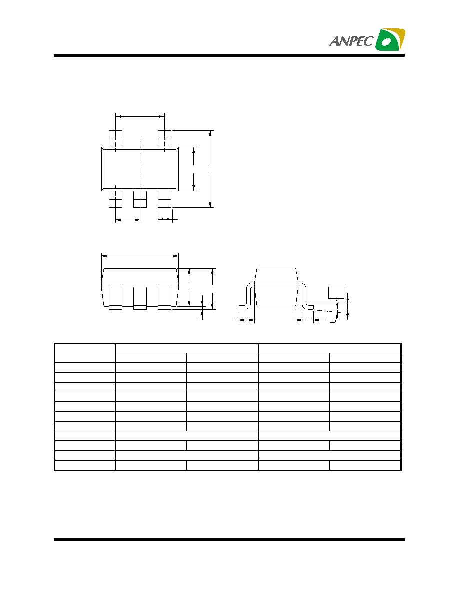
Packaging Information
SOT-23-5
e 1
E 1
E
b
1
2
3
4
5
e
D
A 2
A
A 1
L 2
L
L 1
a
M i l l i m e t e r s
I n c h e s
D i m
M i n .
M a x .
M i n .
M a x .
A
0 . 9 5
1 . 4 5
0 . 0 3 7
0 . 0 5 7
A 1
0 . 0 5
0 . 1 5
0 . 0 0 2
0 . 0 0 6
A 2
0 . 9 0
1 . 3 0
0 . 0 3 5
0 . 0 5 1
D
2 . 8
3 . 0 0
0 . 11 0
0 . 11 8
E
2 . 6
3 . 0 0
0 . 1 0 2
0 . 11 8
E 1
1 . 5
1 . 7 0
0 . 0 5 9
0 . 0 6 7
L
0 . 3 5
0 . 5 5
0 . 0 1 4
0 . 0 2 2
L 1
0 . 2 0 B S C
0 . 0 0 8 B SC
L 2
0 . 5
0 . 7
0 . 0 2 0
0 . 0 2 8
N
5
5
0
∞
1 0
∞
0
∞
1 0
∞
Copyright
ANPEC Electronics Corp.
Rev. B.1 - Mar., 2004
APL5301/2
www.anpec.com.tw
15
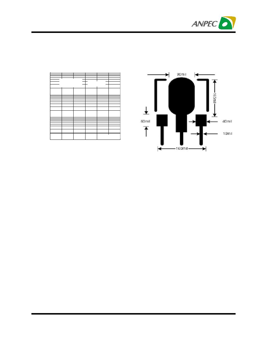
SOT-89 (Reference EIAJ ED-7500A Reg stration SC-62)
Packaging Information
D
D 1
e
B 1
e 1
B
1
2
3
L
H
E
C
a
a
A
M illim eters
Inches
D im
M in.
M ax.
M in.
M ax.
A
1.40
1.60
0.055
0.063
B
0.40
0.56
0.016
0.022
B 1
0.35
0.48
0.014
0.019
C
0.35
0.44
0.014
0.017
D
4.40
4.60
0.173
0.181
D 1
1.35
1.83
0.053
0.072
e
1.50 B SC
0.059 BSC
e1
3.00 B SC
0.118 B SC
E
2.29
2.60
0.090
0.102
H
3.75
4.25
0.148
0.167
L
0.80
1.20
0.031
0.047
10
∞
10
∞
Copyright
ANPEC Electronics Corp.
Rev. B.1 - Mar., 2004
APL5301/2
www.anpec.com.tw
16
Packaging Information
SOT-89-5
M illim eters
Inches
D im
M in.
M ax.
M in.
M ax.
A
4.40
4.60
0.17
0.18
B
4.05
4.25
0.16
0.17
C
1.50
1.70
0.06
0.07
D
1.30
1.50
0.05
0.06
E
2.40
2.60
0.09
0.1
F
0.80
-
0.03
-
G
3.00 R EF
0.12 R EF
H
1.50 R EF
0.06 R EF
I
0.40
0.52
0.01
0.02
J
1.40
1.60
0.05
0.06
K
0.35
0.41
0.01
0.02
L
5 TY P
0.2 TYP
Copyright
ANPEC Electronics Corp.
Rev. B.1 - Mar., 2004
APL5301/2
www.anpec.com.tw
17
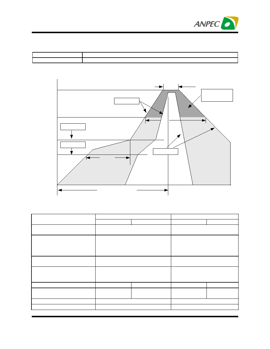
t 25 C to P e ak
tp
R am p-u p
t
L
R am p-d ow n
ts
P rehea t
T sm ax
T sm in
T
L
T
P
25
Tem
p
er
at
ur
e
T im e
C ritical Z one
T
L
to T
P
∞
Physical Specifications
Terminal Material
Solder-Plated Copper (Solder Material : 90/10 or 63/37 SnPb), 100%Sn
Lead Solderability
Meets EIA Specification RSI86-91, ANSI/J-STD-002 Category 3.
Reflow Condition
(IR/Convection or VPR Reflow)
Classificatin Reflow Profiles
Sn-Pb Eutectic Assembly
Pb-Free Assembly
Profile Feature
Large Body
Small Body
Large Body
Small Body
Average ramp-up rate
(T
L
to T
P
)
3
∞
C/second max.
3
∞
C/second max.
Preheat
-
Temperature Min (Tsmin)
-
Temperature Mix (Tsmax)
-
Time (min to max)(ts)
100
∞
C
150
∞
C
60-120 seconds
150
∞
C
200
∞
C
60-180 seconds
Tsmax to T
L
- Ramp-up Rate
3
∞
C/second max
Tsmax to T
L
-
Temperature(T
L
)
-
Time (t
L
)
183
∞
C
60-150 seconds
217
∞
C
60-150 seconds
Peak Temperature(Tp)
225 +0/-5
∞
C 240
+0/-5
∞
C 245
+0/-5
∞
C 250
+0/-5
∞
C
Time within 5
∞
C of actual Peak
Temperature(tp)
10-30 seconds
10-30 seconds
10-30 seconds 20-40 seconds
Ramp-down Rate
6
∞
C/second max.
6
∞
C/second max.
Time 25
∞
C to Peak Temperature
6 minutes max.
8 minutes max.
Note: All temperatures refer to topside of the package. Measured on the body surface.
Copyright
ANPEC Electronics Corp.
Rev. B.1 - Mar., 2004
APL5301/2
www.anpec.com.tw
18
R e lia b ility te s t p ro g ra m
Te s t ite m
M e th o d
D e s c rip tio n
S O L D E R A B IL IT Y
M IL -S T D -8 8 3 D -2 0 0 3
2 4 5
∞
C , 5 S E C
H O LT
M IL -S T D -8 8 3 D -1 0 0 5 .7
1 0 0 0 H rs B ia s @ 1 2 5
∞
C
P C T
J E S D -2 2 - B , A 1 0 2
1 6 8 H rs , 1 0 0 % R H , 1 2 1
∞
C
T S T
M IL -S T D -8 8 3 D -1 0 11 .9
-6 5
∞
C ~ 1 5 0
∞
C , 2 0 0 C y c le s
E S D
M IL -S T D -8 8 3 D -3 0 1 5 .7
V H B M > 2 K V, V M M > 2 0 0 V
L a tc h -U p
J E S D 7 8
1 0 m s , I
tr
> 1 0 0 m A
Carrier Tape
A
J
B
T 2
T 1
C
t
A o
E
W
P o
P
K o
B o
D 1
D
F
P 1
Copyright
ANPEC Electronics Corp.
Rev. B.1 - Mar., 2004
APL5301/2
www.anpec.com.tw
19
A p p lic a tion
A
B
C
J
T 1
T 2
W
P
E
3 30
±
1
6 2 + 1.5
1 2.7 5+
0 .1 5
2
±
0 .5
1 2.4
±
0.2
2
±
0 .2
1 2
±
0 . 3
8
±
0 .1
1 .7 5
±
0 .1
F
D
D 1
P o
P 1
A o
B o
K o
t
S O P - 8
5 .5
±
1
1 .5 5 + 0.1
1 .5 5 + 0.2 5
4 .0
±
0 .1
2 .0
±
0 .1
6 .4
±
0 .1
5 .2
±
0 . 1
2 .1
±
0 .1
0 .3
±
0 .01 3
A p p lic a tion
A
B
C
J
T 1
T 2
W
P
E
1 78
±
1
7 0
±
2
1 3.5
±
0.15
3
±
0 .1 5
1 4
±
2
1 .3
±
0 .3
1 2 + 0.3
1 2 - 0 .1
8
±
0 .1
1 .7 5
±
0 .1
F
D
D 1
P o
P 1
A o
B o
K o
t
S O T -89
5 .5
±
0 .05
1 .5
±
0 .1
1 .5
±
0 .1
4 .0
±
0 .1
2 .0
±
0 .1
4 .8
±
0 .1
4 .5
±
0 .1
1 .8 0
±
0 .1
0 .3
±
0 .01 3
A p p lic a tion
A
B
C
J
T 1
T 2
W
P
E
1 78
±
1
7 2
±
1 .0
1 3.0 + 0 .2
2 .5
±
0 .15
8 .4
±
2
1 .5
±
0 .3
8 .0 + 0.3
- 0.3
4
±
0 .1
1 .7 5
±
0 .1
F
D
D 1
P o
P 1
A o
B o
K o
t
S O T -23 -5
3 .5
±
0 .05
1 .5 + 0.1
1 .5 + 0.1
4 .0
±
0 .1
2 .0
±
0 .1
3 .1 5
±
0.1
3 .2
±
0 .1
1 .4
±
0 .1
0 .2
±
0 .03
Cover Tape Dimensions
Anpec Electronics Corp.
Head Office :
5F, No. 2 Li-Hsin Road, SBIP,
Hsin-Chu, Taiwan, R.O.C.
Tel : 886-3-5642000
Fax : 886-3-5642050
Taipei Branch :
7F, No. 137, Lane 235, Pac Chiao Rd.,
Hsin Tien City, Taipei Hsien, Taiwan, R. O. C.
Tel : 886-2-89191368
Fax : 886-2-89191369
Customer Service
Reel Dimensions
Application
Carrier Width
Cover Tape Width
Devices Per Reel
SOP- 8
12
9.3
2500
SOT- 23
8
5.3
3000
SOT- 89
12
9.3
1000
(mm)