 | ÐлекÑÑоннÑй компоненÑ: APM2313A | СкаÑаÑÑ:  PDF PDF  ZIP ZIP |
Äîêóìåíòàöèÿ è îïèñàíèÿ www.docs.chipfind.ru
P-Channel Enhancement Mode MOSFET
Copyright
ANPEC Electronics Corp.
Rev. A.1 - Jun., 2003
www.anpec.com.tw
1
ANPEC reserves the right to make changes to improve reliability or manufacturability without notice, and advise customers to obtain
the latest version of relevant information to verify before placing orders.
APM2313
Ordering and Marking Information
Features
Applications
Absolute Maximum Ratings
(T
A
= 25
°
C unless otherwise noted)
·
-20V/-1.8A , R
DS(ON)
=108m
(typ.) @ V
GS
=-4.5V
R
DS(ON)
=135m
(typ.) @ V
GS
=-2.5V
··
··
·
Super High Dense Cell Design for Extremely
Low R
DS(ON)
··
··
·
Reliable and Rugged
··
··
·
SOT-23 Package
·
Power Management in Notebook Computer ,
Portable Equipment and Battery Powered
Systems.
A P M 2313
H andling C ode
T em p. R an ge
P a ckage C o de
P a ckage C o de
A : S O T -23
O perating Junction T em p. R ange
C : -55 to 1 50 C
H andling C ode
T R : T ape & R eel
°
A P M 2313 A :
M 13X
X - D ate C ode
Symbol
Parameter
Rating
Unit
V
DSS
Drain-Source Voltage
-20
V
GSS
Gate-Source Voltage
±10
V
I
D
*
Maximum Drain Current Continuous
-1.8
I
DM
Maximum Drain Current Pulsed
-7
A
* Surface Mounted on FR4 Board, t
10 sec.
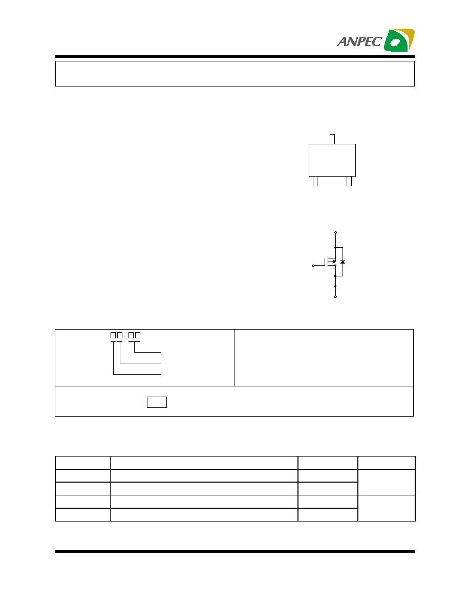
Pin Description
G
D
S
Top View of SOT-23
P-Channel MOSFET
G
S
D
Copyright
ANPEC Electronics Corp.
Rev. A.1 - Jun., 2003
www.anpec.com.tw
2
APM2313
Notes
a
: Pulse test ; pulse width
300
µ
s, duty cycle
2
%
b
: Guaranteed by design, not subject to production testing
Absolute Maximum Ratings (Cont.)
(T
A
= 25
°
C unless otherwise noted)
Symbol
Parameter
Rating
Unit
T
A
=25
°
C
1.25
P
D
Maximum Power Dissipation
T
A
=100
°
C
0.5
W
T
J
Maximum Junction Temperature
150
°
C
T
STG
Storage Temperature Range
-55 to 150
°
C
R
jA
Thermal Resistance Junction to Ambient
100
°
C/W
APM2313
Symbol
Parameter
Test Condition
Min.
Typ.
Max.
Unit
Static
BV
DSS
Drain-Source Breakdown
Voltage
V
GS
=0V , I
DS
=-250
µ
A
-20
V
I
DSS
Zero Gate Voltage Drain
Current
V
DS
=-16V , V
GS
=0V
-1
µ
A
V
GS(th)
Gate Threshold Voltage
V
DS
=V
GS
, I
DS
=-250
µ
A
-0.5
-0.7
-1
V
I
GSS
Gate Leakage Current
V
GS
=
±
10V , V
DS
=0V
±
100
nA
V
GS
=-4.5V , I
DS
=-1.8A
108
140
R
DS(ON)
a
Drain-Source On-state
Resistance
V
GS
=-2.5V , I
DS
=-0.8A
135
175
m
V
SD
a
Diode Forward Voltage
I
SD
=-0.5A , V
GS
=0V
-0.8
-1.3
V
Dynamic
b
Q
g
Total Gate Charge
5.3
7
Q
gs
Gate-Source Charge
1.04
Q
gd
Gate-Drain Charge
V
DS
=-10V , I
DS
= -1.8A ,
V
GS
=-4.5V
0.62
nC
t
d(ON)
Turn-on Delay Time
8
16
T
r
Turn-on Rise Time
7
15
t
d(OFF)
Turn-off Delay Time
18
35
T
f
Turn-off Fall Time
V
DD
=-10V , I
DS
=-1A ,
V
GEN
=-4.5V , R
G
=6
8
15
ns
C
iss
Input Capacitance
435
C
oss
Output Capacitance
120
C
rss
Reverse Transfer Capacitance
V
GS
=0V
V
DS
=-15V
Frequency=1.0MHz
65
pF
Electrical Characteristics
(T
A
= 25
°
C unless otherwise noted)
Copyright
ANPEC Electronics Corp.
Rev. A.1 - Jun., 2003
www.anpec.com.tw
3
APM2313
0
1
2
3
4
5
0
1
2
3
4
5
6
7
0.0
0.5
1.0
1.5
2.0
2.5
0
1
2
3
4
5
6
7
0
1
2
3
4
5
6
7
0.08
0.09
0.10
0.11
0.12
0.13
0.14
0.15
0.16
0.17
0.18
-50 -25
0
25
50
75
100 125 150
0.00
0.25
0.50
0.75
1.00
1.25
1.50
1.75
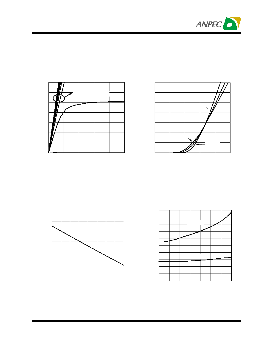
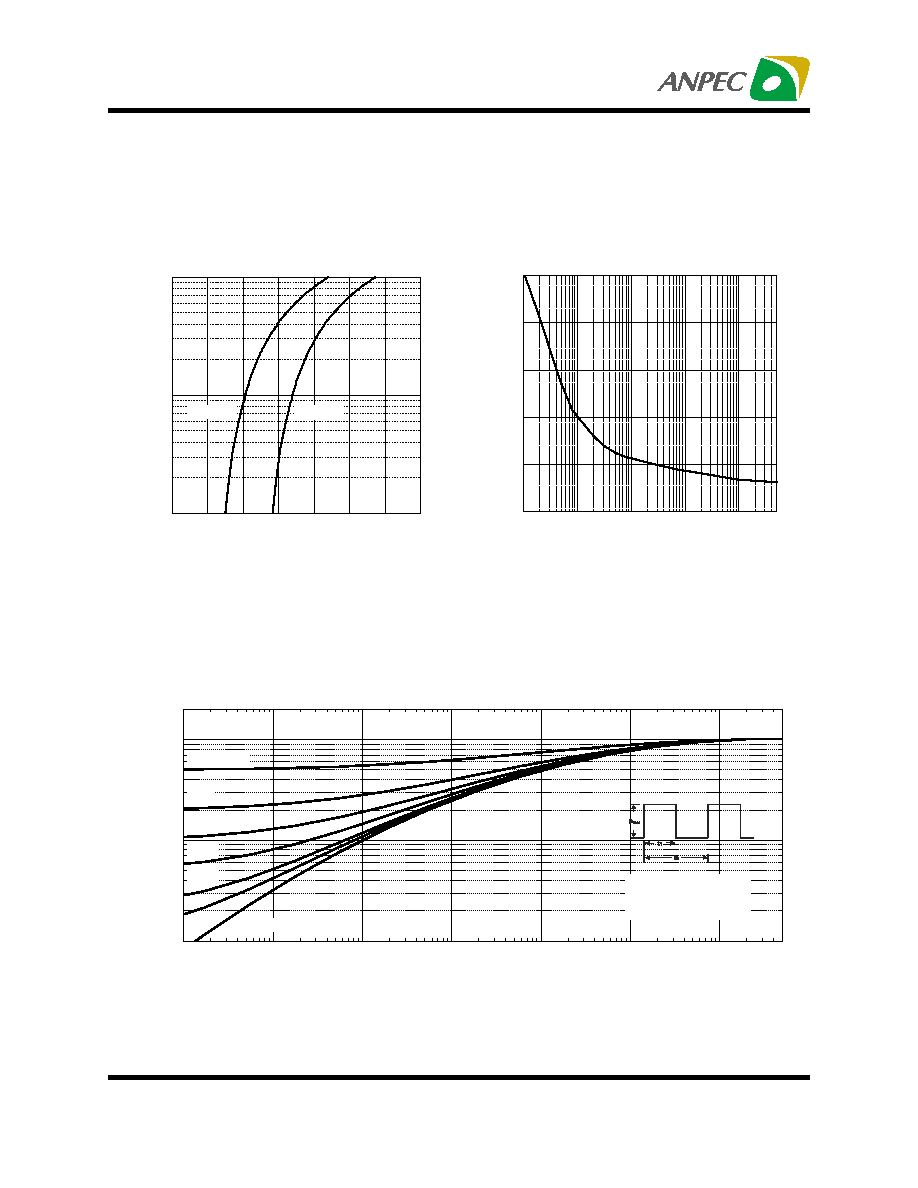
Typical Characteristics
-I
D-
Drain Current (A)
Transfer Characteristics
T
J
=-55°C
T
J
=25°C
T
J
=125°C
-V
GS
- Gate-to-Source Voltage (V)
Threshold Voltage vs. Junction Temperature
Tj - Junction Temperature (°C)
-V
GS(th)-
Threshold V
oltage (V)
(Normalized)
-I
DS
=250
µ
A
R
DS(ON)
-On-Resistance (
)
On-Resistance vs. Drain Current
-V
GS
=2.5V
-I
D
- Drain Current (A)
-V
GS
=4.5V
-V
GS
=1V
Output Characteristics
-I
D
-Drain Current (A)
-V
GS
=3,4,5,6,7,8,9,10V
-V
GS
=2V
-V
DS
- Drain-to-Source Voltage (V)
Copyright
ANPEC Electronics Corp.
Rev. A.1 - Jun., 2003
www.anpec.com.tw
4
APM2313
0
5
10
15
20
0
100
200
300
400
500
600
1
2
3
4
5
6
7
8
9
10
0.06
0.07
0.08
0.09
0.10
0.11
0.12
0.13
0.14
0.15
0.16
0
1
2
3
4
5
6
0
1
2
3
4
5
-50
-25
0
25
50
75
100 125 150
0.0
0.5
1.0
1.5
2.0
2.5
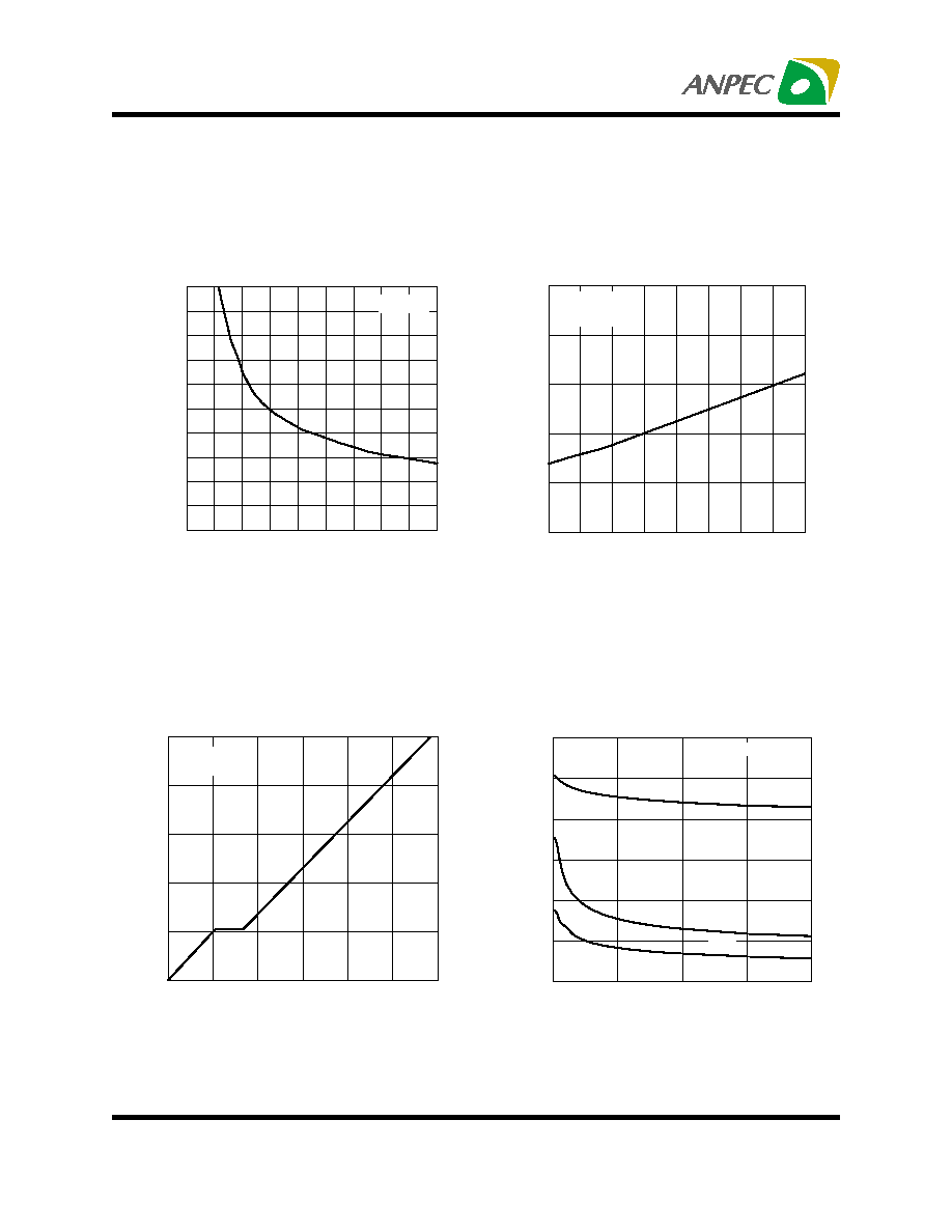
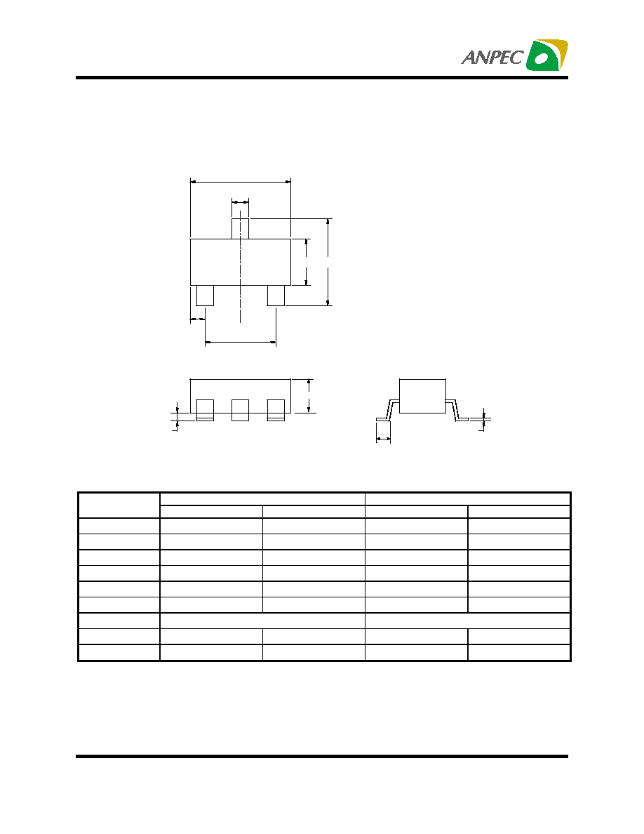
Typical Characteristics (Cont.)
R
DS(ON)
-On-Resistance (
)
(Normalized)
On-Resistance vs. Junction Temperature
-V
GS
=4.5V
-I
D
=1.8A
T
J
- Junction Temperature (°C)
-V
DS
- Drain-to-Source Voltage (V)
Capacitance
Capacitance (pF)
Ciss
Coss
Crss
-V
GS
- Gate-to-Source Voltage (V)
R
DS(ON)
-On-Resistance (
)
-I
D
=1.8A
On-Resistance vs. Gate-to-Source Voltage
Gate Charge
Q
G
- Gate Charge (nC)
-V
GS
-Gate-Source V
oltage (V)
-V
DS
=10V
-I
D
=1.8A
Frequency=1MHz
Copyright
ANPEC Electronics Corp.
Rev. A.1 - Jun., 2003
www.anpec.com.tw
5
APM2313
1E-4
1E-3
0.01
0.1
1
10
100
0.01
0.1
1
500
0.01
0.1
1
10
100
0
2
4
6
8
10
500
0.0
0.3
0.6
0.9
1.2
1.5
1.8
2.1
0.1
1
10
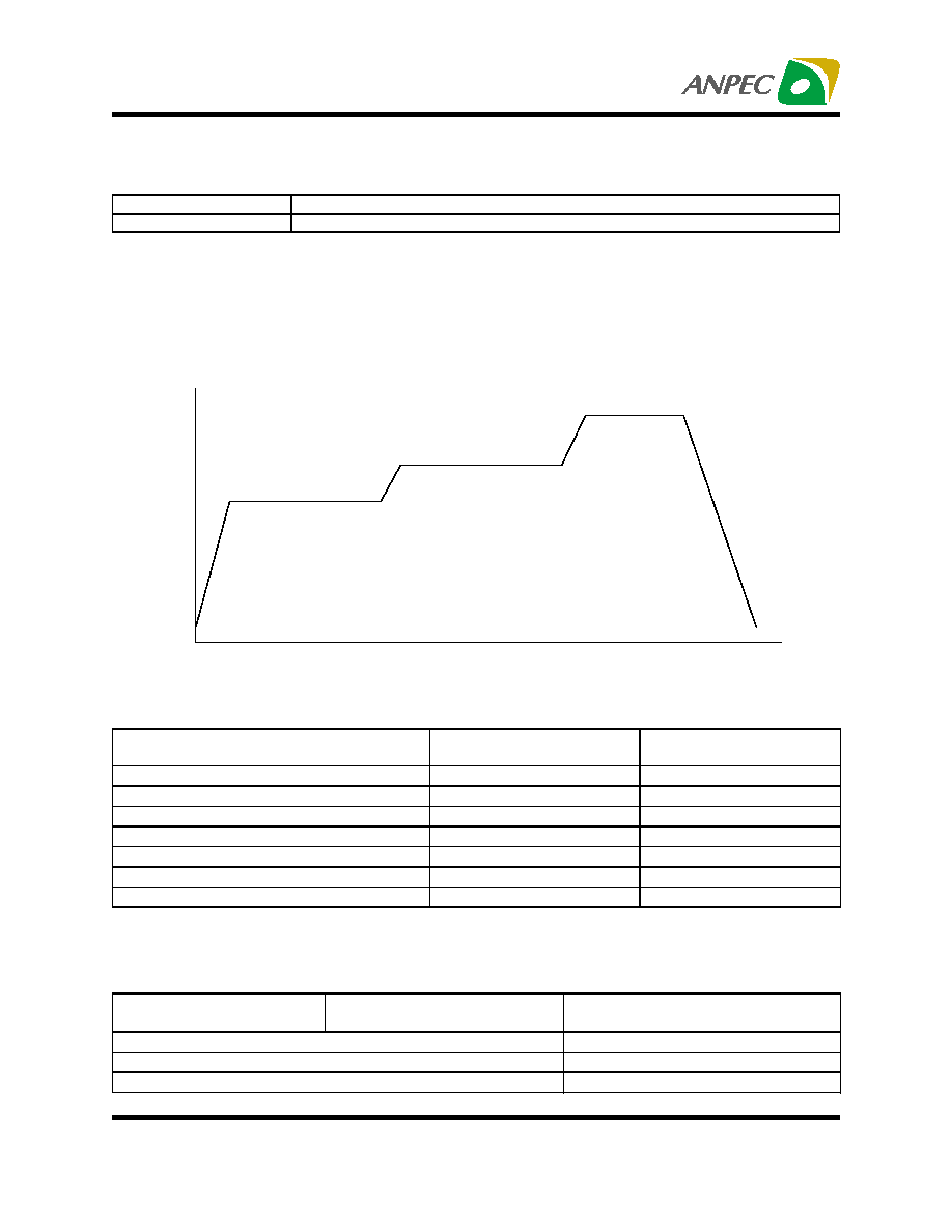
Typical Characteristics (Cont.)
Power (W)
Single Pulse Power
Time (sec)
Square Wave Pulse Duration (sec)
Source-Drain Diode Forward Voltage
-I
S
-Source Current (A)
T
J
=150°C
T
J
=25°C
-V
SD
-Source-to-Drain Voltage (V)
Normalized Effective Transient
Thermal Impedance
Normalized Thermal Transient Impedence, Junction to Ambient
1.Duty Cycle, D=t1/t2
2.Per Unit Base=R
thJA
=100°C/W
3.T
JM
-T
A
=P
DM
Z
thJA
Duty Cycle=0.5
D=0.2
D=0.1
D=0.05
D=0.02
SINGLE PULSE
D=0.01
Copyright
ANPEC Electronics Corp.
Rev. A.1 - Jun., 2003
www.anpec.com.tw
6
APM2313
Packaging Information
D
E
H
S
e
A
A1
L
C
B
3
2
1
M illimet ers
Inches
Dim
M in.
M ax.
M in.
M ax.
A
1.00
1.30
0.039
0.051
A1
0.00
0.10
0.000
0.004
B
0.35
0.51
0.014
0.020
C
0.10
0.25
0.004
0.010
D
2.70
3.10
0.106
0.122
E
1.40
1.80
0.055
0.071
e
1.90 BSC
0.075 BSC
H
2.40
3.00
0.094
0.118
L
0.37
0.0015
SOT-23
Copyright
ANPEC Electronics Corp.
Rev. A.1 - Jun., 2003
www.anpec.com.tw
7
APM2313
Reference JEDEC Standard J-STD-020A APRIL 1999
Reflow Condition
(IR/Convection or VPR Reflow)
Physical Specifications
Pre-heat temperature
183 C
Peak temperature
Time
°
temperature
Classification Reflow Profiles
Convection or IR/
Convection
VPR
Average ramp-up rate(183
°
C to Peak)
3
°
C/second max.
10
°
C /second max.
Preheat temperature 125 ± 25
°
C)
120 seconds max
Temperature maintained above 183
°
C
60 150 seconds
Time within 5
°
C of actual peak temperature 10 20 seconds
60 seconds
Peak temperature range
220 +5/-0
°
C or 235 +5/-0
°
C 215-219
°
C or 235 +5/-0
°
C
Ramp-down rate
6
°
C /second max.
10
°
C /second max.
Time 25
°
C to peak temperature
6 minutes max.
Package Reflow Conditions
pkg. thickness
2.5mm
and all bgas
pkg. thickness < 2.5mm and
pkg. volume
350 mm³
pkg. thickness < 2.5mm and pkg.
volume < 350mm³
Convection 220 +5/-0
°
C
Convection 235 +5/-0
°
C
VPR 215-219
°
C
VPR 235 +5/-0
°
C
IR/Convection 220 +5/-0
°
C
IR/Convection 235 +5/-0
°
C
Terminal Material
Solder-Plated Copper (Solder Material : 90/10 or 63/37 SnPb)
Lead Solderability
Meets EIA Specification RSI86-91, ANSI/J-STD-002 Category 3.
Copyright
ANPEC Electronics Corp.
Rev. A.1 - Jun., 2003
www.anpec.com.tw
8
APM2313
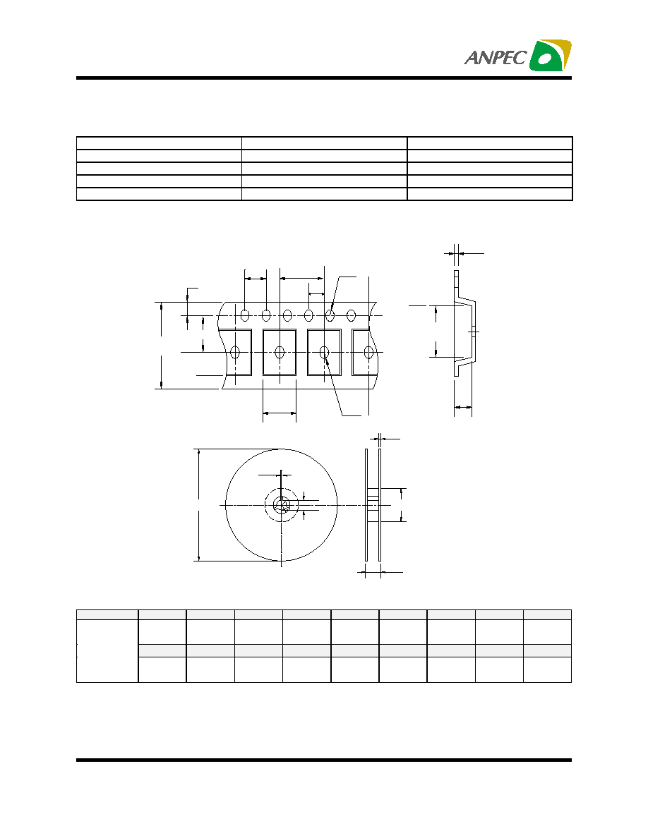
Carrier Tape
A
J
B
T2
T1
C
t
Ao
E
W
Po
P
Ko
Bo
D1
D
F
P1
Application
A
B
C
J
T1
T2
W
P
E
178
±
1
72
±
1.0
13.0 + 0.2 2.5
±
0.15
8.4
±
2
1.5
±
0.3
8.0+ 0.3
- 0.3
4
±
0.1
1.75
±
0.1
F
D
D1
Po
P1
Ao
Bo
Ko
t
SOT-23
3.5
±
0.05 1.5 +0.1
1.5 +0.1
4.0
±
0.1
2.0
±
0.1 3.15
±
0.1 3.2
±
0.1
1.4
±
0.1
0.2
±
0.03
Test item
Method
Description
SOLDERABILITY
MIL-STD-883D-2003
245°C,5 SEC
HOLT
MIL-STD 883D-1005.7
1000 Hrs Bias @ 125°C
PCT
JESD-22-B, A102
168 Hrs, 100% RH, 121°C
TST
MIL-STD 883D-1011.9
-65°C ~ 150°C, 200 Cycles
Reliability test program

Copyright
ANPEC Electronics Corp.
Rev. A.1 - Jun., 2003
www.anpec.com.tw
9
APM2313
Customer Service
Anpec Electronics Corp.
Head Office :
5F, No. 2 Li-Hsin Road, SBIP,
Hsin-Chu, Taiwan, R.O.C.
Tel : 886-3-5642000
Fax : 886-3-5642050
Taipei Branch :
7F, No. 137, Lane 235, Pac Chiao Rd.,
Hsin Tien City, Taipei Hsien, Taiwan, R. O. C.
Tel : 886-2-89191368
Fax : 886-2-89191369
Cover Tape Dimensions
Application
Carrier Width
Cover Tape Width
Devices Per Reel
SOT- 23
8
5.3
3000