 | –≠–ª–µ–∫—Ç—Ä–æ–Ω–Ω—ã–π –∫–æ–º–ø–æ–Ω–µ–Ω—Ç: AO4900AL | –°–∫–∞—á–∞—Ç—å:  PDF PDF  ZIP ZIP |
Symbol
Units
V
DS
V
V
GS
V
T
A
=25∞C
T
A
=70∞C
I
DM
V
KA
V
T
A
=25∞C
T
A
=70∞C
I
FM
T
A
=25∞C
T
A
=70∞C
T
J
, T
STG
∞C
Symbol
Units
R
JL
R
JL
Pulsed Drain Current
B
Junction and Storage Temperature Range
2
W
Schottky reverse voltage
30
1.44
1.44
Power Dissipation
Max
∞C/W
∞C/W
MOSFET
30
±12
6.9
5.8
40
2
I
F
40
Thermal Characteristics Schottky
62.5
48
55
90
Continuous Drain Current
A
Gate-Source Voltage
Schottky
Drain-Source Voltage
Parameter
-55 to 150
A
Absolute Maximum Ratings T
A
=25∞C unless otherwise noted
P
D
I
D
3
A
2
40
Continuous Forward Current
A
Parameter: Thermal Characteristics MOSFET
Maximum Junction-to-Ambient
A
t 10s
-55 to 150
Typ
Maximum Junction-to-Ambient
A
Steady-State
110
Maximum Junction-to-Lead
C
Steady-State
40
62.5
Maximum Junction-to-Ambient
A
t 10s
R
JA
Maximum Junction-to-Ambient
A
Steady-State
110
Maximum Junction-to-Lead
C
Steady-State
Pulsed Forward Current
B
71
32
47.5
R
JA
AO4900A
Dual N-Channel Enhancement Mode Field Effect Transistor
with Schottky Diode
Features
V
DS
(V) = 30V
I
D
= 6.9A (V
GS
= 10V)
R
DS(ON)
< 27m
(V
GS
= 10V)
R
DS(ON)
< 32m
(V
GS
= 4.5V)
R
DS(ON)
< 50m
(V
GS
= 2.5V)
SCHOTTKY
V
DS
(V) = 30V, I
F
= 3A, V
F
=0.5V@1A
General Description
The AO4900A uses advanced trench technology to
provide excellent R
DS(ON)
and low gate charge. The
two MOSFETs make a compact and efficient switch
and synchronous rectifier combination for use in DC-
DC converters. A Schottky diode is co-packaged in
parallel with the synchronous MOSFET to boost
efficiency further.
Standard Product AO4900A is Pb-
free (meets ROHS & Sony 259 specifications).
AO4900AL is a Green Product ordering option.
AO4900A and AO4900AL are electrically identical.
SOIC-8
G1
S1
G2
S2/A
D1
D1
D2/K
D2/K
1
2
3
4
8
7
6
5
G2
D2
S2
K
A
G1
D1
S1
Alpha & Omega Semiconductor, Ltd.
AO4900A
Symbol
Min
Typ
Max
Units
BV
DSS
30
V
0.002
1
T
J
=55∞C
5
I
GSS
100
nA
V
GS(th)
0.7
1
1.5
V
I
D(ON)
40
A
20
27
T
J
=125∞C
25
40
23
32
m
34
50
m
g
FS
10
26
S
V
SD
0.71
1
V
I
S
4.5
A
C
iss
900
1100
pF
C
oss
88
pF
C
rss
65
pF
R
g
0.95
1.5
Q
g
10
12
nC
Q
gs
1.8
nC
Q
gd
3.75
nC
t
D(on)
3.2
ns
t
r
3.5
ns
t
D(off)
21.5
ns
t
f
2.7
ns
t
rr
16.8
20
ns
Q
rr
8
12
nC
SCHOTTKY PARAMETERS
V
F
0.45
0.5
V
0.007
0.05
3.2
10
12
20
C
T
37
pF
THIS PRODUCT HAS BEEN DESIGNED AND QUALIFIED FOR THE CONSUMER MARKET. APPLICATIONS OR USES AS CRITICAL
COMPONENTS IN LIFE SUPPORT DEVICES OR SYSTEMS ARE NOT AUTHORIZED. AOS DOES NOT ASSUME ANY LIABILITY ARISING
OUT OF SUCH APPLICATIONS OR USES OF ITS PRODUCTS. AOS RESERVES THE RIGHT TO IMPROVE PRODUCT DESIGN,
FUNCTIONS AND RELIABILITY WITHOUT NOTICE.
mA
V
R
=30V, T
J
=125∞C
V
R
=30V, T
J
=150∞C
Junction Capacitance
V
R
=15V
Forward Voltage Drop
I
F
=1.0A
I
rm
Maximum reverse leakage current
V
R
=30V
Body Diode Reverse Recovery Time
Body Diode Reverse Recovery Charge I
F
=5A, dI/dt=100A/
µs
Drain-Source Breakdown Voltage
On state drain current
I
D
=250
µA, V
GS
=0V
V
GS
=2.5V, I
D
=5A
V
GS
=4.5V, V
DS
=5V
V
GS
=10V, I
D
=6.9A
Reverse Transfer Capacitance
Electrical Characteristics (T
J
=25∞C unless otherwise noted)
STATIC PARAMETERS
Parameter
Conditions
I
DSS
µA
Gate Threshold Voltage
V
DS
=V
GS
I
D
=250
µA
V
DS
=24V, V
GS
=0V
V
DS
=0V, V
GS
= ±12V
Zero Gate Voltage Drain Current
Gate-Body leakage current
R
DS(ON)
Static Drain-Source On-Resistance
Forward Transconductance
Diode Forward Voltage
I
F
=5A, dI/dt=100A/
µs
V
GS
=0V, V
DS
=15V, f=1MHz
SWITCHING PARAMETERS
Total Gate Charge
V
GS
=4.5V, V
DS
=15V, I
D
=8.5A
Gate Source Charge
Gate Drain Charge
Turn-On Rise Time
Turn-Off DelayTime
V
GS
=10V, V
DS
=15V, R
L
=1.8
,
R
GEN
=6
Turn-Off Fall Time
Maximum Body-Diode Continuous Current
Input Capacitance
Output Capacitance
Turn-On DelayTime
DYNAMIC PARAMETERS
Gate resistance
V
GS
=0V, V
DS
=0V, f=1MHz
m
V
GS
=4.5V, I
D
=6A
I
S
=1A,V
GS
=0V
V
DS
=5V, I
D
=5A
A: The value of R
JA
is measured with the device mounted on 1in
2
FR-4 board with 2oz. Copper, in a still air environment with T
A
=25∞C. The
value in any given application depends on the user's specific board design. The current rating is based on the t 10s thermal resistance
rating.
B: Repetitive rating, pulse width limited by junction temperature.
C. The R
JA
is the sum of the thermal impedence from junction to lead R
JL
and lead to ambient.
D. The static characteristics in Figures 1 to 6 are obtained using 80
µs pulses, duty cycle 0.5% max.
E. These tests are performed with the device mounted on 1 in
2
FR-4 board with 2oz. Copper, in a still air environment with T
A
=25∞C. The SOA
curve provides a single pulse rating.
Rev 0 : Feb 2006
Alpha & Omega Semiconductor, Ltd.
AO4900A
TYPICAL ELECTRICAL AND THERMAL CHARACTERISTICS
THIS PRODUCT HAS BEEN DESIGNED AND QUALIFIED FOR THE CONSUMER MARKET. APPLICATIONS OR USES AS CRITICAL
COMPONENTS IN LIFE SUPPORT DEVICES OR SYSTEMS ARE NOT AUTHORIZED. AOS DOES NOT ASSUME ANY LIABILITY ARISING
OUT OF SUCH APPLICATIONS OR USES OF ITS PRODUCTS. AOS RESERVES THE RIGHT TO IMPROVE PRODUCT DESIGN,
FUNCTIONS AND RELIABILITY WITHOUT NOTICE.
0
10
20
30
40
50
60
0
1
2
3
4
5
V
DS
(Volts)
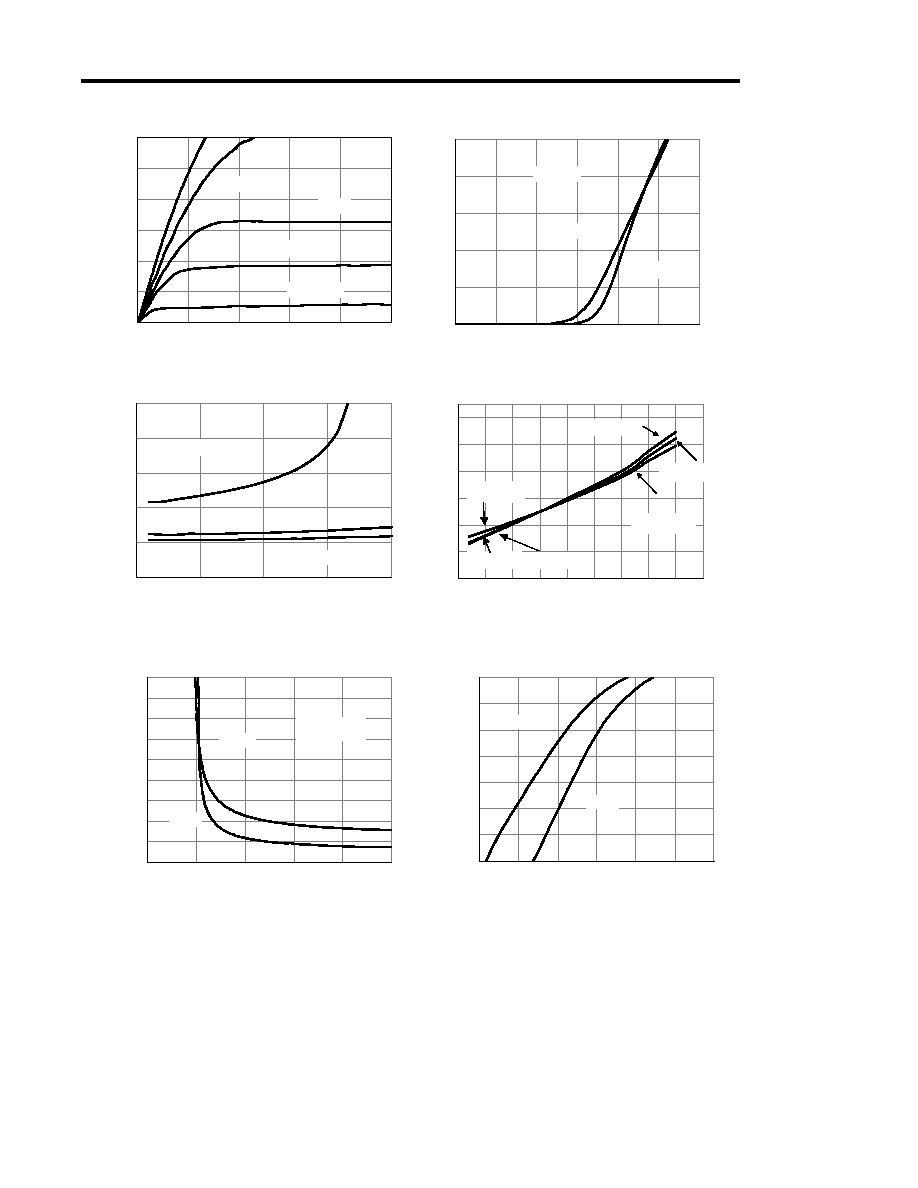
Fig 1: On-Region Characteristics
I
D
(A
)
V
GS
=2V
2.5V
3V
4.5V
10V
0
4
8
12
16
20
0
0.5
1
1.5
2
2.5
3
V
GS
(Volts)
Figure 2: Transfer Characteristics
I
D
(A
)
10
20
30
40
50
60
0
5
10
15
20
I
D
(A)
Figure 3: On-Resistance vs. Drain Current and
Gate Voltage
R
DS(
O
N)
(m
)
1.0E-06
1.0E-05
1.0E-04
1.0E-03
1.0E-02
1.0E-01
1.0E+00
1.0E+01
0.0
0.2
0.4
0.6
0.8
1.0
1.2
V
SD
(Volts)
Figure 6: Body-Diode Characteristics
I
S
(A
)
25∞C
125∞C
0.5
0.7
0.9
1.1
1.3
1.5
1.7
-50
-25
0
25
50
75
100 125 150 175
Temperature (∞C)
Figure 4: On-Resistance vs. Junction
Temperature
N
o
r
m
aliz
ed
O
n
-
R
esist
an
ce
V
GS
=2.5V
V
GS
=10V
V
GS
=4.5V
V
GS
=4.5
V
GS
=10V
V
GS
=2.5V
10
20
30
40
50
60
70
80
90
100
0
2
4
6
8
10
V
GS
(Volts)
Figure 5: On-Resistance vs. Gate-Source Voltage
R
DS(
O
N)
(m
)
25∞C
125∞C
V
DS
=5V
V
GS
=2.5V
V
GS
=4.5V
V
GS
=10V
I
D
=6.9A
25∞C
125∞C
Alpha & Omega Semiconductor, Ltd.
AO4900A
TYPICAL ELECTRICAL AND THERMAL CHARACTERISTICS
THIS PRODUCT HAS BEEN DESIGNED AND QUALIFIED FOR THE CONSUMER MARKET. APPLICATIONS OR USES AS CRITICAL
COMPONENTS IN LIFE SUPPORT DEVICES OR SYSTEMS ARE NOT AUTHORIZED. AOS DOES NOT ASSUME ANY LIABILITY ARISING
OUT OF SUCH APPLICATIONS OR USES OF ITS PRODUCTS. AOS RESERVES THE RIGHT TO IMPROVE PRODUCT DESIGN,
FUNCTIONS AND RELIABILITY WITHOUT NOTICE.
0
1
2
3
4
5
0
2
4
6
8
10
12
Q
g
(nC)
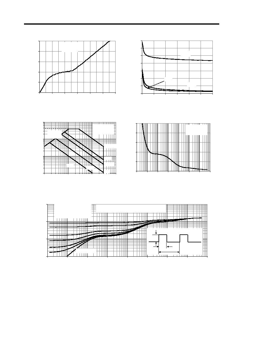
Figure 7: Gate-Charge Characteristics
V
GS
(V
ol
ts
)
0
200
400
600
800
1000
1200
1400
0
5
10
15
20
25
30
V
DS
(Volts)
Figure 8: Capacitance Characteristics
C
a
p
acit
a
n
ce (
p
F
)
C
iss
0
10
20
30
40
50
0.0001 0.001
0.01
0.1
1
10
100
1000
Pulse Width (s)
Figure 10: Single Pulse Power Rating Junction-to-
Ambient (Note E)
Po
w
e
r (
W
)
0.01
0.1
1
10
0.00001
0.0001
0.001
0.01
0.1
1
10
100
1000
Pulse Width (s)
Figure 11: Normalized Maximum Transient Thermal Impedance
Z
JA
N
o
r
m
aliz
ed
T
r
an
sien
t
T
h
e
r
m
al R
esist
an
ce
C
oss
C
rss
V
DS
=15V
I
D
=6.9A
Single Pulse
D=T
on
/T
T
J,PK
=T
A
+P
DM
.Z
JA
.R
JA
R
JA
=62.5∞C/W
T
on
T
P
D
In descending order
D=0.5, 0.3, 0.1, 0.05, 0.02, 0.01, single pulse
T
J(Max)
=150∞C
T
A
=25∞C
0.1
1.0
10.0
100.0
0.1
1
10
100
V
DS
(Volts)
I
D
(A
mps
)
Figure 9: Maximum Forward Biased Safe
Operating Area (Note E)
10
µs
10ms
1ms
1s
10s
DC
R
DS(ON)
limited
T
J(Max)
=150∞C
T
A
=25∞C
Alpha & Omega Semiconductor, Ltd.
AO4900A
TYPICAL ELECTRICAL AND THERMAL CHARACTERISTICS: SCHOTTKY
0.001
0.01
0.1
1
10
0.0
0.2
0.4
0.6
0.8
1.0
1.2
V
F
(Volts)
Figure 12: Schottky Forward Characteristics
I
F
(A
mps
)
0
50
100
150
200
250
0
5
10
15
20
25
30
V
KA
(Volts)
Figure 13: Schottky Capacitance Characteristics
C
a
p
acit
a
n
ce (
p
F
)
0.001
0.01
0.1
1
10
100
0
25
50
75
100
125
150
175
Temperature (∞C)
Figure 15: Schottky Leakage current vs. Junction
Temperature
L
eakag
e C
u
r
r
e
n
t
(
m
A
)
0.01
0.1
1
10
0.00001
0.0001
0.001
0.01
0.1
1
10
100
1000
Pulse Width (s)
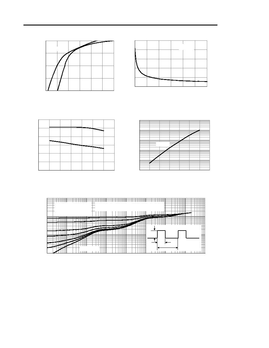
Figure 15: Schottky Normalized Maximum Transient Thermal Impedance
Z
JA
N
o
r
m
aliz
ed
T
r
an
sien
t
T
h
e
r
m
al R
esist
an
ce
0.1
0.2
0.3
0.4
0.5
0.6
0.7
0
25
50
75
100
125
150
175
Temperature (∞C)
V
F
(V
ol
ts
)
Figure 14: Schottky Forward Drop vs.
Junction Temperature
Single Pulse
D=T
on
/T
T
J,PK
=T
A
+P
DM
.Z
JA
.R
JA
R
JA
=62.5∞C/W
In descending order
D=0.5, 0.3, 0.1, 0.05, 0.02, 0.01, single pulse
f = 1MHz
I
F
=1A
25∞C
I
F
=3A
V
R
=30V
125∞C
T
on
T
P
D
Alpha & Omega Semiconductor, Ltd.