 | –≠–ª–µ–∫—Ç—Ä–æ–Ω–Ω—ã–π –∫–æ–º–ø–æ–Ω–µ–Ω—Ç: AO7401 | –°–∫–∞—á–∞—Ç—å:  PDF PDF  ZIP ZIP |
Symbol
V
DS
V
GS
I
DM
T
J
, T
STG
Symbol
Typ
Max
300
360
350
425
R
JL
280
320
W
Maximum Junction-to-Lead
C
Steady-State
∞C/W
Thermal Characteristics
Parameter
Units
Maximum Junction-to-Ambient
A
t 10s
R
JA
∞C/W
Maximum Junction-to-Ambient
A
Steady-State
∞C/W
±12
Gate-Source Voltage
Drain-Source Voltage
-30
Continuous Drain
Current
A
Maximum
Units
Parameter
T
A
=25∞C
T
A
=70∞C
Absolute Maximum Ratings T
A
=25∞C unless otherwise noted
V
V
-1.0
-10
Pulsed Drain Current
B
Power Dissipation
A
T
A
=25∞C
Junction and Storage Temperature Range
A
P
D
∞C
0.35
0.22
-55 to 150
T
A
=70∞C
I
D
-1.2
AO7401
P-Channel Enhancement Mode Field Effect Transistor
Nov 2002
Features
V
DS
(V) = -30V
I
D
= -1.2A
R
DS(ON)
< 150m
(V
GS
= -10V)
R
DS(ON)
< 200m
(V
GS
= -4.5V)
R
DS(ON)
< 280m
(V
GS
= -2.5V)
General Description
The AO7401 uses advanced trench technology to
provide excellent R
DS(ON)
, low gate charge, and
operation with gate voltages as low as 2.5V, in the
small SOT323 footprint. It can be used for a wide
variety of applications, including load switching, low
current inverters and low current DC-DC converters.
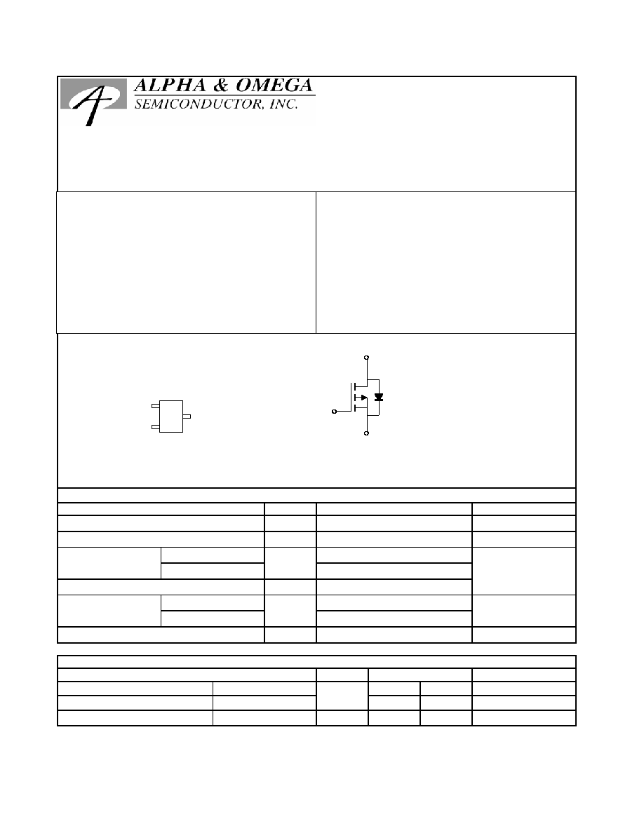
G
D
S
S
G
D
SC-70
(SOT-323)
Top View
Alpha & Omega Semiconductor, Ltd.

AO7401
Symbol
Min
Typ
Max
Units
BV
DSS
-30
V
-1
T
J
=55∞C
-5
I
GSS
±100
nA
V
GS(th)
-0.6
-1
-1.4
V
I
D(ON)
-10
A
122
150
T
J
=125∞C
173
220
147
200
m
207
280
m
g
FS
3
4.5
S
V
SD
-0.85
-1
V
I
S
-0.5
A
C
iss
409
pF
C
oss
55
pF
C
rss
42
pF
R
g
12
Q
g
5.06
nC
Q
gs
0.72
nC
Q
gd
1.58
nC
t
D(on)
6.2
ns
t
r
3.2
ns
t
D(off)
41.2
ns
t
f
14.5
ns
t
rr
13.2
ns
Q
rr
5.4
nC
Gate resistance
V
GS
=0V, V
DS
=0V, f=1MHz
Turn-Off Fall Time
Maximum Body-Diode Continuous Current
Input Capacitance
Output Capacitance
Turn-On DelayTime
DYNAMIC PARAMETERS
I
F
=-1A, dI/dt=100A/
µs
V
GS
=0V, V
DS
=-15V, f=1MHz
SWITCHING PARAMETERS
Total Gate Charge
V
GS
=-4.5V, V
DS
=-15V, I
D
=-1A
Gate Source Charge
Gate Drain Charge
Turn-On Rise Time
Turn-Off DelayTime
V
GS
=-10V, V
DS
=-15V, R
L
=15
,
R
GEN
=3
m
V
GS
=-4.5V, I
D
=-1.2A
I
S
=-1A,V
GS
=0V
V
DS
=-5V, I
D
=-1.2A
R
DS(ON)
Static Drain-Source On-Resistance
Forward Transconductance
Diode Forward Voltage
I
DSS
µA
Gate Threshold Voltage
V
DS
=V
GS
I
D
=-250
µA
V
DS
=-24V, V
GS
=0V
V
DS
=0V, V
GS
=±12V
Zero Gate Voltage Drain Current
Gate-Body leakage current
Electrical Characteristics (T
J
=25∞C unless otherwise noted)
STATIC PARAMETERS
Parameter
Conditions
Body Diode Reverse Recovery Time
Body Diode Reverse Recovery Charge I
F
=-1A, dI/dt=100A/
µs
Drain-Source Breakdown Voltage
On state drain current
I
D
=-250
µA, V
GS
=0V
V
GS
=-2.5V, I
D
=-1A
V
GS
=-4.5V, V
DS
=-5V
V
GS
=-10V, I
D
=-1.2A
Reverse Transfer Capacitance
A: The value of R
JA
is measured with the device mounted on 1in
2
FR-4 board with 2oz. Copper, in a still air environment with T
A
=25∞C. The
value in any a given application depends on the user's specific board design. The current rating is based on the t
10s thermal resistance
rating.
B: Repetitive rating, pulse width limited by junction temperature.
C. The R
JA
is the sum of the thermal impedence from junction to lead R
JL
and lead to ambient.
D. The static characteristics in Figures 1 to 6,12,14 are obtained using 80
µs pulses, duty cycle 0.5% max.
E. These tests are performed with the device mounted on 1 in
2
FR-4 board with 2oz. Copper, in a still air environment with T
A
=25∞C. The
SOA curve provides a single pulse rating.
Alpha & Omega Semiconductor, Ltd.
AO
7401
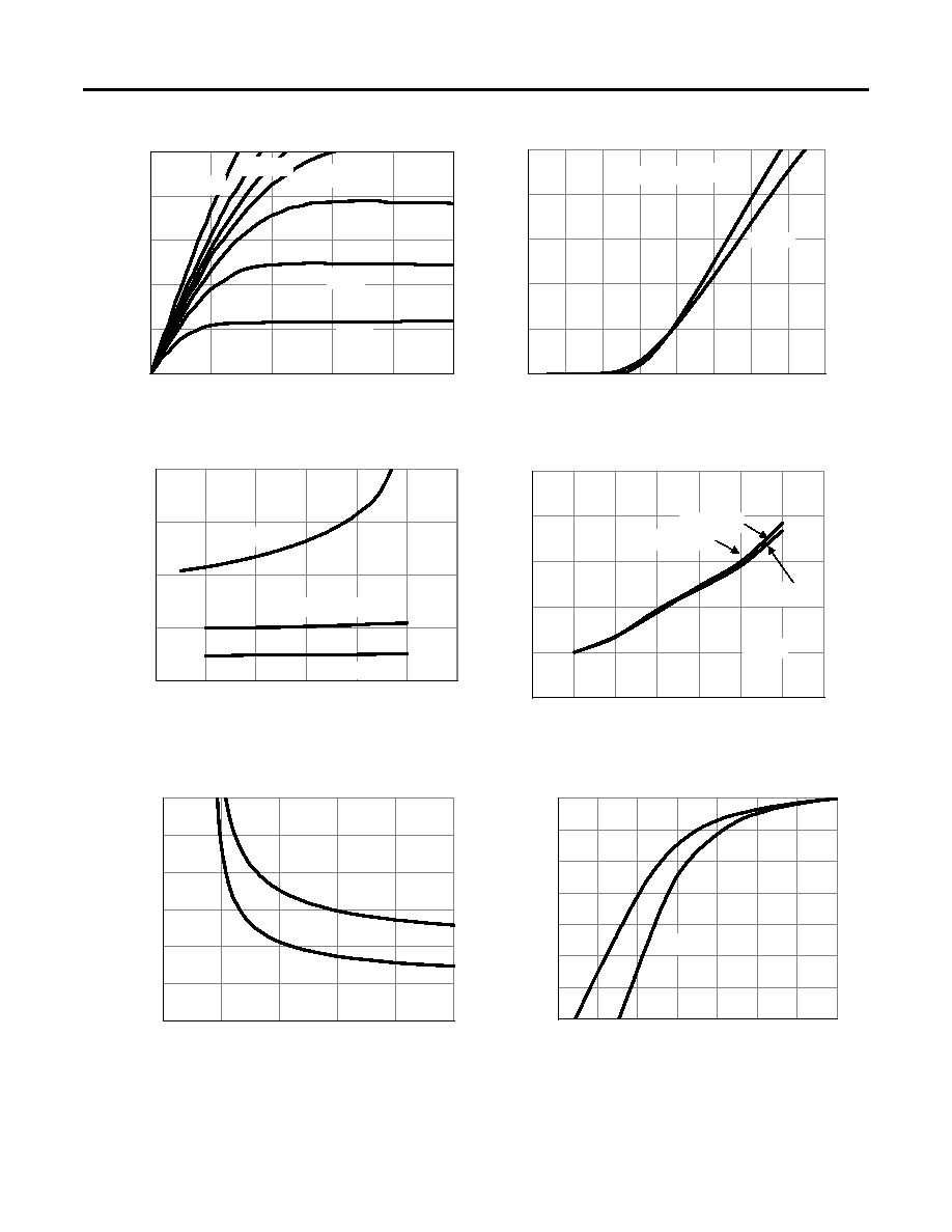
TYPICAL ELECTRICAL AND THERMAL CHARACTERISTICS
0
2
4
6
8
10
0
1
2
3
4
5
-V
DS
(Volts)
Fig 1: On-Region Characteristics
-I
D
(A)
V
GS
=-3.5V
-2.0V
-3V
-5V
-10V
0
2
4
6
8
10
0
0.5
1
1.5
2
2.5
3
3.5
4
-V
GS
(Volts)
Figure 2: Transfer Characteristics
-I
D
(A)
100
150
200
250
300
0
1
2
3
4
5
6
-I
D
(A)
Figure 3: On-Resistance vs. Drain Current and Gate
Voltage
R
DS
(
O
N)
(m
)
1.0E-06
1.0E-05
1.0E-04
1.0E-03
1.0E-02
1.0E-01
1.0E+00
1.0E+01
0.0
0.2
0.4
0.6
0.8
1.0
1.2
1.4
-V
SD
(Volts)
Figure 6: Body-Diode Characteristics
-I
S
(A)
25∞C
125∞C
0.8
1
1.2
1.4
1.6
1.8
0
25
50
75
100
125
150
175
Temperature (∞C)
Figure 4: On-Resistance vs. Junction Temperature
N
o
r
mal
i
z
ed
O
n
-
R
esi
st
an
ce
V
GS
=-10V
V
GS
=-2.5V
50
100
150
200
250
300
350
0
2
4
6
8
10
-V
GS
(Volts)
Figure 5: On-Resistance vs. Gate-Source Voltage
R
DS
(
O
N)
(m
)
25∞C
125∞C
V
DS
=-5V
V
GS
=-4.5V
V
GS
=-10V
I
D
=-1A
25∞C
125∞C
I
D
=-1A
-4V
V
GS
=-2.5V
V
GS
=-4.5V
-2.5V
Alpha and Omega Semiconductor, Ltd.
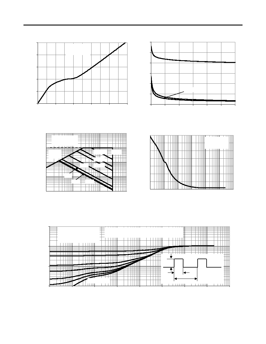
AO
7401
TYPICAL ELECTRICAL AND THERMAL CHARACTERISTICS
0
1
2
3
4
5
0
1
2
3
4
5
-Q
g
(nC)
Figure 7: Gate-Charge Characteristics
-V
GS
(Vo
l
ts
)
0
100
200
300
400
500
600
0
5
10
15
20
25
30
-V
DS
(Volts)
Figure 8: Capacitance Characteristics
C
ap
aci
t
an
ce (
p
F
)
C
iss
0
2
4
6
8
10
12
14
0.001
0.01
0.1
1
10
100
1000
Pulse Width (s)
Figure 10: Single Pulse Power Rating Junction-to-
Ambient (Note E)
Pow
e
r
(W)
0.01
0.1
1
10
0.00001
0.0001
0.001
0.01
0.1
1
10
100
1000
Pulse Width (s)
Figure 11: Normalized Maximum Transient Thermal Impedance
Z
JA
N
o
r
mal
i
z
ed
T
r
an
si
en
t
T
h
er
mal
R
esi
st
an
ce
C
oss
C
rss
0.01
0.10
1.00
10.00
100.00
0.1
1
10
100
-V
DS
(Volts)
-I
D
(Am
p
s
)
Figure 9: Maximum Forward Biased Safe
Operating Area (Note E)
100
µs
10ms
1ms
0.1s
1s
10s
DC
R
DS(ON)
limited
T
J(Max)
=150∞C
T
A
=25∞C
V
DS
=-15V
I
D
=-1A
Single Pulse
D=T
on
/T
T
J,PK
=T
A
+P
DM
.Z
JA
.R
JA
R
JA
=360∞C/W
T
on
T
P
D
In descending order
D=0.5, 0.3, 0.1, 0.05, 0.02, 0.01, single pulse
T
J(Max)
=150∞C
T
A
=25∞C
10
µs
Alpha & Omega Semiconductor, Ltd.

NOTE:
1. LEAD FINISH: 150 MICROINCHES ( 3.8 um) MIN.
THICKNESS OF Tin/Lead (SOLDER) PLATED ON LEAD
2. TOLERANCE ±0.10 mm (4 mil) UNLESS OTHERWISE
SPECIFIED
3. COPLANARITY : 0.10 mm
4. OTHER NAME OF THIS PACKAGE IS CALLED SOT-323
SC-70 3L Package Data
RECOMMENDATION OF LAND PATTERN
P N W
NOTE:
P - PART NUMBER CODE.
N - FOUNDRY AND ASSEMBLY LOCATION CODE
W - YAER AND WEEK CODE.
L T - ASSEMBLY LOT CODE.
CODE
AO7401
1
PART NO.
SC-70 3L PART NO. CODE
PACKAGE MARKING DESCRIPTION
Rev. A
0.10
0.00
A1
1.00
0.20
0.40
1.35
0.40
2.20
2.20
0.30
0.65 BSC
e
1∞
0.10
L
1
e1
1.30 BSC
8∞
0.25
0.90
0.10
0.30
2.00
1.15
1.80
D
E1
F
E
b
C
A2
1.10
MAX
DIMENSIONS IN MILLIMETERS
SYMBOLS
0.90
MIN
A
L T