 | –≠–ª–µ–∫—Ç—Ä–æ–Ω–Ω—ã–π –∫–æ–º–ø–æ–Ω–µ–Ω—Ç: AOZ1013AI | –°–∫–∞—á–∞—Ç—å:  PDF PDF  ZIP ZIP |
^lwNMNP=
EZBuckTM 3A Simple Buck Regulator
February 2006
February 2006
w w w . a o s m d . c o m
Page 1 of 16
General Description
The AOZ1013 is a high efficiency, simple to use, 3A buck
regulator. The AOZ1013 works from a 4.5V to 16V input
voltage range, and provides up to 3A of continuous output
current with an output voltage adjustable down to 0.8V.
The AOZ1013 comes in SO-8 packages and is rated over a
-40∞C to +85∞C ambient temperature range.
Features
∑ 4.5V to 16V operating input voltage range
∑ 50 m internal PFET switch for high
efficiency: up to 95%
∑ Internal soft start
∑ Output voltage adjustable to 0.8V
∑ 3A continuous output current
∑ Fixed 500kHz PWM operation
∑ Cycle-by-cycle current limit
∑ Short-circuit protection
∑ Thermal shutdown
∑ Small size SO-8 packages
Applications
∑ Point of load dc/dc conversion
∑ PCIe graphics cards
∑ Set top boxes
∑ DVD drives and HDD
∑ LCD panels
∑ Cable modems
∑ Telecom/Networking/Datacom equipment
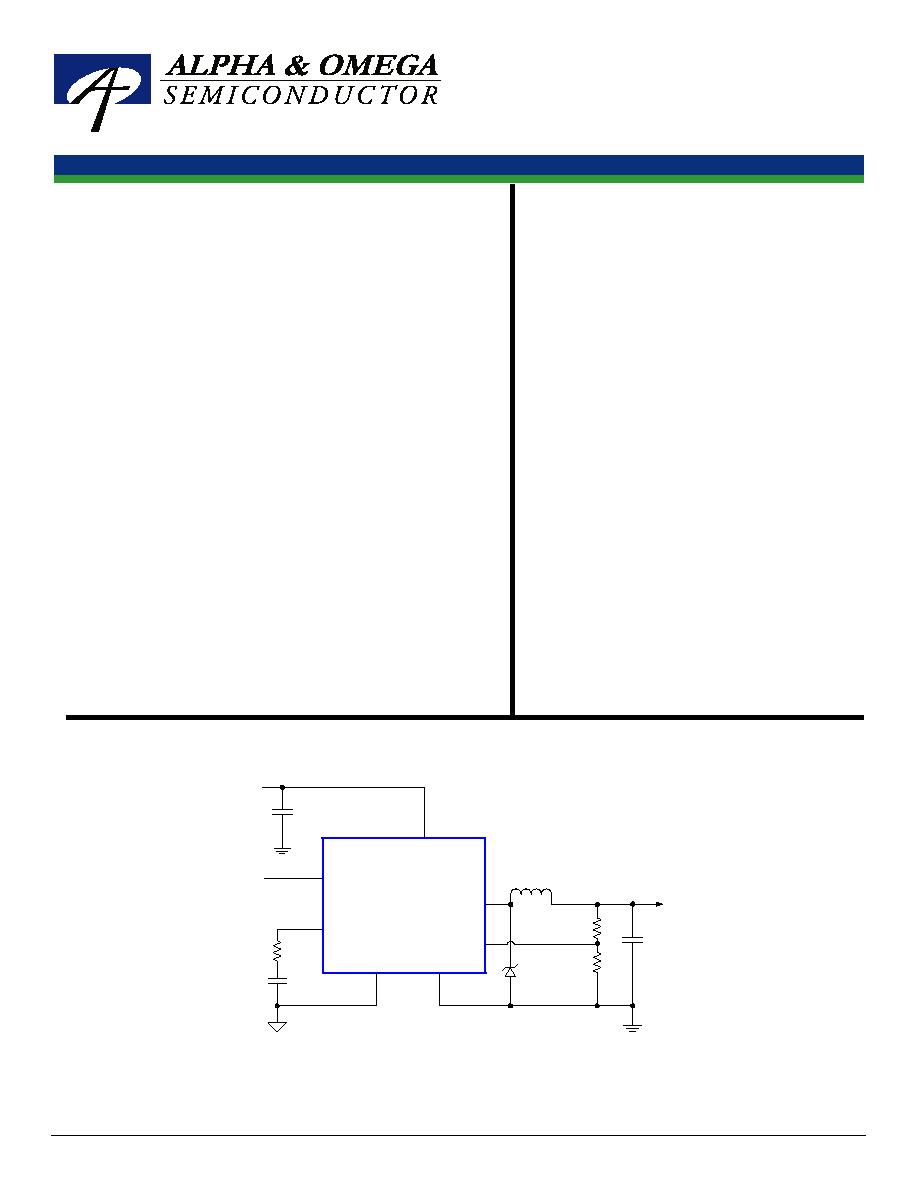
Typical Application
L1
C2
VOUT
AOZ1013
C1
LX
VIN
FB
PGND
COMP
EN
AGND
10uF
47uF
4.7uH
From uPC
R
C
C
C
R1
R2
D1
+3.3V Output
@3A
VIN
Figure 1. 3.3V/3A Buck Down Regulator
^lwNMNP
February 2006
w w w . a o s m d . c o m
Page 2 of 16
Ordering Information
Part Number
Ambient Temperature Range
Package
Environmental
AOZ1013AI
-40∞C to +85∞C
SO-8
RoHS
Pin Configuration
SO-8
1
2
3
4
8
7
6
5
VIN
AGND
COMP
LX
LX
EN
FB
PGND
Pin Description
Pin Number
Pin Name
Pin Function
1
VIN
Supply voltage input. When VIN rises above the UVLO threshold the
device starts up.
2
PGND
Power ground. Electrically needs to be connected to AGND.
3 AGND
Reference
connection
for
controller section. Also used as thermal
connection for controller section. Electrically needs to be connected
to PGND.
4 FB
The FB pin is used to determine the output voltage via a resistor
divider between the output and GND.
5
COMP
External loop compensation pin.
6
EN
The enable pin is active high. Connect EN pin to VIN if not used. Do
not leave the EN pin floating.
7,8
LX
PWM output connection to inductor. Thermal connection for output
stage.
Absolute Maximum Ratings
(1)
Recommend Operating Ratings
(2)
Parameter
Units
Parameter
Units
Supply Voltage (V
IN
)
18V
Supply Voltage (V
IN
)
4.5V to 16V
LX to AGND
-0.7V to V
IN
+0.3V
Output Voltage Range
0.8V to V
IN
EN to AGND
-0.3V to V
IN
+0.3V
Ambient Temperature (T
A
)
-40∞C to +85∞C
FB to AGND
-0.3V to 6V
COMP to AGND
-0.3V to 6V
Package Thermal Resistance
SO-8 (
JA
)
82∞ C/W
PGND to AGND
-0.3V to +0.3V
Junction Temperature (T
J
) +150∞C
Storage Temperature (T
S
) -65∞C
to
+150∞C
ESD Rating(3)
2kV
^lwNMNP
February 2006
w w w . a o s m d . c o m
Page 3 of 16
Electrical Characteristics
T
A
= 25∞C, V
IN
= V
EN
= 12V, V
OUT
= 3.3V unless otherwise specified.
Parameter
Symbol
Conditions
MIN
TYP
MAX
UNITS
Supply Voltage
V
IN
4.5 16
V
Input Under-Voltage Lockout
Threshold
V
UVLO
V
IN
rising
V
IN
falling
4.00
3.70
V
V
Supply Current (Quiescent)
I
IN
I
OUT
= 0, V
FB
= 1.2V,
V
EN
>2V
2
3
mA
Shutdown Supply Current
I
OFF
V
EN
= 0V
3 20
µ
A
Feedback Voltage
V
FB
0.782
0.8
0.818 V
Load Regulation
0.5
%
Line Regulation
1
%
Feedback Voltage Input Current
I
FB
200 nA
EN Input Threshold
V
EN
Off
threshold
On threshold
2.0
0.6
V
V
EN Input Hysteresis
V
HYS
100
mV
Modulator
Frequency f
O
350
500
600 kHz
Maximum Duty Cycle
D
MAX
100
%
Minimum Duty Cycle
D
MIN
6
%
Error Amplifier Voltage Gain
500
V/V
Error Amplifier Transconductance
200
µ
A/V
Protection
Current Limit
I
LIM
4
5
A
Over-Temperature Shutdown
Limit
T
J
rising
T
J
falling
145
100
∞C
∞C
Soft Start Interval
t
SS
4
ms
Output Stage
High-Side Switch On-Resistance
V
IN
= 12V
V
IN
= 5V
40
65
50
85
m
m
Notes:
1.
Exceeding the Absolute Maximum ratings may damage the device.
2.
The device is not guaranteed to operate beyond the Maximum Operating ratings.
3.
Devices are inherently ESD sensitive, handling precautions are required. Human body model rating: 1.5K
in series
with 100pF.
4.
Specification in BOLD indicate an ambient temperature range of -40∞C to +85∞C. These specifications are guaranteed
by design.
^lwNMNP
February 2006
w w w . a o s m d . c o m
Page 4 of 16
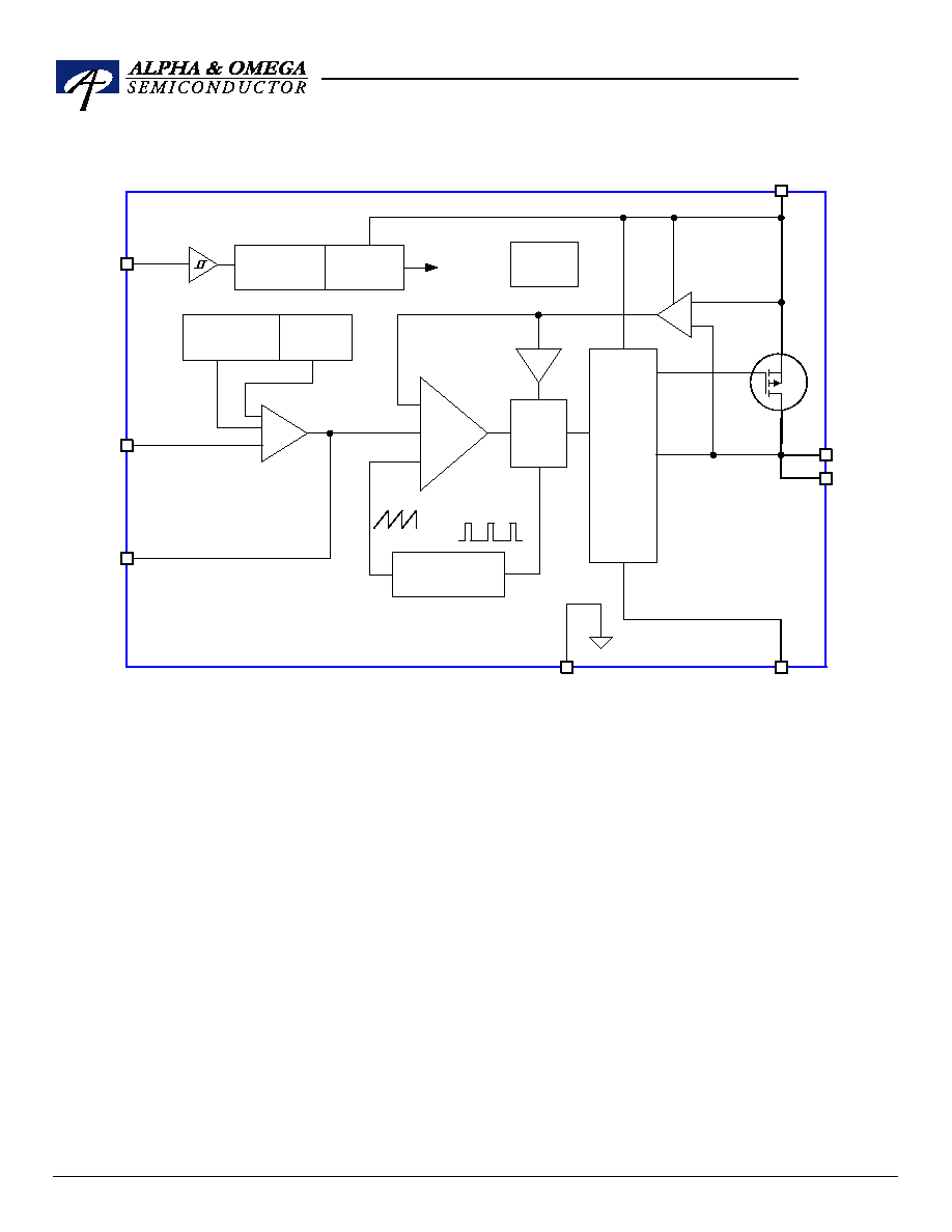
Functional Block Diagram
LE
V
E
L S
H
I
FTE
R
+
F
E
T DRI
V
E
R
500Khz
OSCILLATOR
UVLO
&
POR
LX
FB
PGND
COMP
EN
AGND
+
-
PWM
CONTROL
LOGIC
+
≠
+
ISEN
ILIMIT
PWM
COMP
5V LDO
REGULATOR
+
-
EAMP
Internal +5V
REFERENCE
&
BIAS
OTP
SOFTSTART
0.8V
LX
Vin
Q1
^lwNMNP
February 2006
w w w . a o s m d . c o m
Page 5 of 16
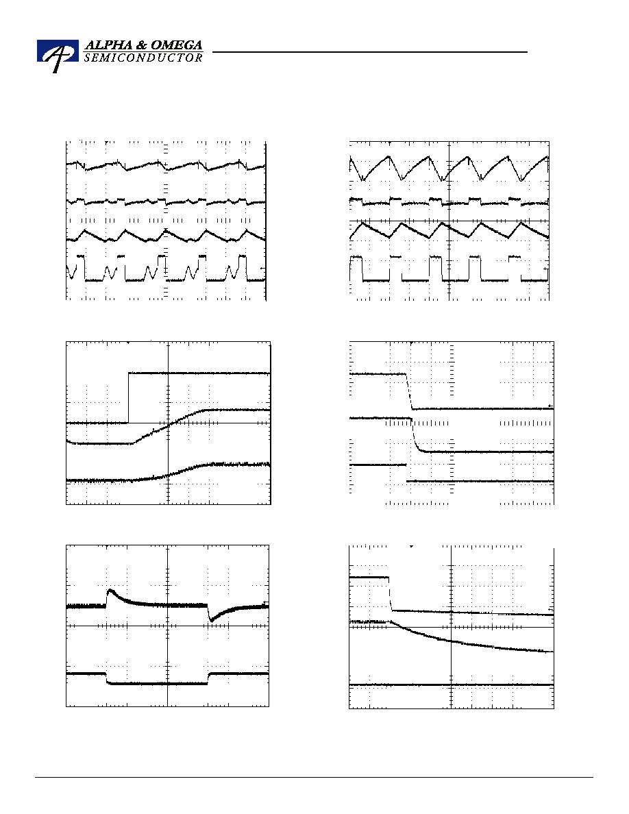
Typical Performance Characteristics
Circuit of figure 1. T
A
= 25∞C, V
IN
= V
EN
= 12V, V
OUT
= 3.3V unless otherwise specified.
Light load (DCM) operation
Vin
ripple
50mV/div
Vo
ripple
50mV/div
Iin
2A/div
VLX
10V/div
1us/div
Start up to full load
Vin
5V/div
Vo
1V/div
Iin
1A/div
1ms/div
Load transient
Vo
Ripple
0.1V/div
Io
2A/div
100us/div
Full load (CCM) operation
Vin
ripple
0.1V/div
Vo
ripple
50mV/div
Iin
2A/div
VLX
10V/div
1us/div
Full load to turn off
Vin
5V/div
Vo
1V/div
Iin
1A/div
1ms/div
Light load to turn off
Vin
5V/div
Vo
1V/div
Iin
1A/div
1s/div