 | –≠–ª–µ–∫—Ç—Ä–æ–Ω–Ω—ã–π –∫–æ–º–ø–æ–Ω–µ–Ω—Ç: EK21 | –°–∫–∞—á–∞—Ç—å:  PDF PDF  ZIP ZIP |
APEX MICROTECHNOLOGY CORPORATION ∑ TELEPHONE (520) 690-8600 ∑ FAX (520) 888-3329 ∑ ORDERS (520) 690-8601 ∑ EMAIL prodlit@apexmicrotech.com
1
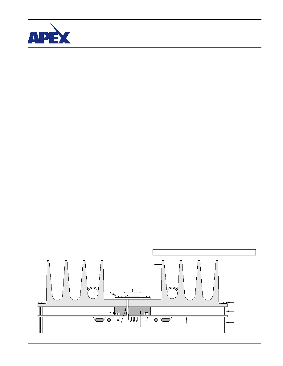
NOTE: Refer to HS11 Heatsink in Accessories section
INTRODUCTION
This easy-to-use kit provides a platform for the evaluation
of power op amps that use the PA74 pin-out configuration. It
can be used to analyze a multitude of standard or proprietary
circuit configurations. In addition, it is flexible enough to do most
standard amplifier test configurations.
The schematic for 1/2 of the PC board is shown in Figure 2.
The schematic for the other half is identical except part refer-
ence designators are primed (i.e. R1 = R1'). Note that all of
the components shown on the schematic will probably not be
used for any single circuit. The component locations on the PC
board (See Figure 3) provide maximum flexibility for a variety
of configurations. Also included are loops for current probes as
well as connection pads on the edge of the PC board for easy
interconnects.
The hardware required to mount the PC board and the device
under evaluation to the heatsink are included in the kit. Because
of the limitless combination of configurations and component
values that can be used, no other parts are included in this kit.
However, generic formulas and guidelines are included in the
APEX DATABOOK and this evaluation kit documentation.
BEFORE YOU GET STARTED
∑ All Apex amplifiers should be handled using proper ESD
precautions!
∑ Initially set all power supplies to the minimum operating levels
allowed in the device data sheet.
∑ Check for oscillations.
∑ Always use the heatsink included in this kit with thermal grease
or a TW03 and torque the part to the specified 4-7 in-lbs
(.45-.79 N∑M).
∑ Do not change connections while the circuit is under pow-
er.
∑ Never exceed any of the absolute maximums listed in the
device data sheet.
∑ Always use adequate power supply bypassing.
∑ Remember that internal power does not equal load power.
∑ Do not count on internal diodes to protect the output against
sustained, high frequency, high energy kickback pulses.
Figure 1
PARTS LIST
Part #
Description
Quantity
HS11
Heatsink
1
EVAL02
PC Board
1
MS03
Mating Socket
2
HWRE01
Hardware Kit
1
TW03
Thermal Washer
1 Box/10
HWRE01 contains the following:
4 #8 Panhead Screw
4 #6 x 1.25" Panhead Screw
4 #8 .375" Hex Spacer
4 #6 x 5/16" Hex Nut
4 #8 1.00" Hex Standoff
2 #6 x 1/4" Hex Nut
ASSEMBLY HINTS
The mating sockets included with this kit have recessed
nut sockets for mounting the device under evaluation. This
allows assembly from one side of the heatsink, making it easy
to swap devices under evaluation. The sizes of the stand-offs
were selected to allow proper spacing of the board-to-heatsink
and allow enough height for components when the assembly
is inverted.
ASSEMBLY
1. Insert a #6 x 5/16" hex nut in each of the nut socket recesses
located on the bottom of the mating socket.
2. Insert the socket into the pc board until it is firmly pressed
against the ground plane side of the pc board.
3. Solder the socket in place (see Figure 1). Be sure the nuts
are in the recesses prior to soldering.
4. Mount the PC board assembly to the heatsink using the
stand-offs and spacers included.
5. Apply thermal grease or a TW03 to the bottom of the device
under evaluation. Insert into the mating socket through the
heatsink.
6. Use the #6 x 1.25" panhead screws to mount the amplifier to
the heat sink. Do not overtorque. Recommended mounting
torque is 4-7 in-lbs (.45-.79 N∑M).
Mounting precautions, general operating considerations,
and heatsinking information may be found in the APEX DATA
BOOK.

APEX MICROTECHNOLOGY CORPORATION ∑ 5980 NORTH SHANNON ROAD ∑ TUCSON, ARIZONA 85741 ∑ USA ∑ APPLICATIONS HOTLINE: 1 (800) 546-2739
2
TYPICAL COMPONENT FUNCTIONS
COMPONENT FUNCTION
R1
Feedback resistor, A side
R2
Input resistor, B side, bridge mode
R3
Feedback resistor, B side
R4
Input resistor, B side
R5
Input resistor, A side
R6
Input bias current measurement (Note 4)
R7
Output current sense resistor or loop for
current probe
R8
Output current sense resistor or loop for
current probe
R9
Input bias current measurement (Note 4)
R10
Noise gain compensation (Note 1)
R11
Resistor divider network for single supply
bias (Note 2)
R12
Resistor divider network for single supply
bias (Note 2)
R13
Noise gain compensation (Note 1)
R14
Input bias current measurement
R15
Input bias current measurement
R16
Resistor divider network for single supply
bias (Note 2)
R17
Resistor divider network for single supply
bias (Note 2)
C1
Input coupling
C2
AC gain set
C3
AC gain or stability (Note 1)
C4
Power supply bypass
C5
Power supply bypass
C6
AC gain or stability (Note 1)
C7
AC gain set
C8
Input coupling
C9
Noise gain compensation (Note 1)
C10
Noise gain compensation (Note 1)
C11
Power supply bypass (Note 3)
C12
Power supply bypass (Note 3)
D1,2,3,4
Flyback protection (Note 5)
C13-16
Bias node noise bypass (Note 2)
EK21
EVALUATION KIT
FOR PA74 PIN-OUT
Figure 2
Figure 3.

APEX MICROTECHNOLOGY CORPORATION ∑ TELEPHONE (520) 690-8600 ∑ FAX (520) 888-3329 ∑ ORDERS (520) 690-8601 ∑ EMAIL prodlit@apexmicrotech.com
3
EK21
Figure 4
Dual
Supply
Bridge
EVALUATION KIT
FOR PA74 PIN-OUT
Figure 5
Single
Supply
Bridge
across the load. To set the gain of the circuit you must deter-
mine the desired voltage across the load at Vin = full scale.
Inserting these values into the following equation will yield the
ratio of R1 to R5.
(V
AB
/(2*Vin)) = R1/R5
The values of R 1,2,3, and 5 should be chosen such that
input bias current will not cause an error voltage that is unac-
ceptable. Set R2 equal to R3 to configure the slave amplifier
as a unity gain inverter.
Figure 5 shows a typical single supply bridge circuit for an AC
coupled input signal. DC coupled inputs may require a different
topology to accommodate proper gain and offset terms for a
desired transfer function.
The gain and output voltage capability for the single supply
bridge are determined the same way as the dual supply bridge
(see AN#2). The difference is the bias requirement for the slave
amplifier. The noninverting input of the slave amplifier should
be biased at mid supply, and must be bypassed.
BRIDGE MODE OPERATION
There are two types of bridge mode operation that will be
covered in this section; dual (or split) supply and single supply.
The PA74 is well suited for both types of bridge mode opera-
tion. If another vendor's pin compatible part is to be compared
to the PA74, a close look at output swing and input common
mode range is in order. The features that make the PA74 an
excellent choice for bridge operation are not included in most
other amplifiers. A lack of common mode range may cause
permanent damage to other pin compatible parts and the in-
ability of other amplifiers to swing close to the supply rails may
cause a lack of available output voltage at the load as well as
increase internal dissipation.
The circuit shown in Figure 4 is a dual supply bridge using
the "master-slave" configuration. Resistors R 6,7,8,9,14,15
and J1 should be shorts. The available output voltage swing
is Vss≠(2*Vsat). If operating a PA74A at 3 Amps and 30 Volts
total supply this translates to:
V
AB
(max) = 30≠(2*3.5) = 23
Of course this 23 volts may be applied in either direction

APEX MICROTECHNOLOGY CORPORATION ∑ 5980 NORTH SHANNON ROAD ∑ TUCSON, ARIZONA 85741 ∑ USA ∑ APPLICATIONS HOTLINE: 1 (800) 546-2739
4
This data sheet has been carefully checked and is believed to be reliable, however, no responsibility is assumed for possible inaccuracies or omissions. All specifications are subject to change without notice.
EK21U REV I JANUARY 2005 © 2005 Apex Microtechnology Corp.
HS11 HEATSINK NOTE
The HS11 Heatsink is provided in this evaluation kit to
guar-
antee adequate thermal design through heat removal from
the part under evaluation. Once maximum power dissipation
for the application is determined (refer to "General Operating
Considerations" and Application Note 11 in the APEX DATA
BOOK), the final mechanical design will probably require sub-
stantially less heatsinking.
APEX MICROTECHNOLOGY makes no representation that
the use or interconnection of the circuits described herein will not
infringe on existing or future patent rights, nor do the descriptions
contained herein imply the granting of licenses to make, use or
sell equipment constructed in accordance therewith.
EK21
EVALUATION KIT
FOR PA74 PIN-OUT
NOTES:Refer to the following sections of the APEX DATA BOOK as noted.
1. See Stability section of "General Operating Considerations."
2. See "Gen. Operating Considerations," and AN3 "Bridge Circuit Drives."
3. See Power Supplies section of "General Operating Considerations."
4. See "Parameter Definitions and Test Methods."
5. See Amplifier Protection section of "Gen. Operating Considerations."