 | –≠–ª–µ–∫—Ç—Ä–æ–Ω–Ω—ã–π –∫–æ–º–ø–æ–Ω–µ–Ω—Ç: MP230 | –°–∫–∞—á–∞—Ç—å:  PDF PDF  ZIP ZIP |

APEX MICROTECHNOLOGY CORPORATION ∑ TELEPHONE (520) 690-8600 ∑ FAX (520) 888-3329 ∑ ORDERS (520) 690-8601 ∑ EMAIL prodlit@apexmicrotech.com
1
FEATURES
∑ LOW COST
∑ HIGH VOLTAGE - 100 VOLTS
∑ HIGH OUTPUT CURRENT - 30 AMPS
∑ 210 WATT DISSIPATION CAPABILITY
APPLICATIONS
∑ MOTOR DRIVE
∑ MAGNETIC DEFLECTION
∑ PROGRAMMABLE POWER SUPPLIES
∑ INDUSTRIAL AUDIO AMPLIFIER
DESCRIPTION
The MP230 operational amplifier is a surface mount con-
structed component that provides a cost effective solution in
many industrial applications. The MP230 offers outstanding
performance that rivals many much more expensive hybrid
components yet has a footprint of only 4.7 sq in. The MP230
has many optional features such as four-wire current limit sens-
ing, a shutdown control and external compensation. In addition,
the class A/B output stage biasing can be turned off for lower
quiescent current with class C operation in applications where
crossover distortion is less important such as when driving motors,
for example. A boost voltage feature biases the output stage for
close linear swings to the supply rail for extra efficient operation.
The MP230 is built on a thermally conductive but electrically
insulating substrate that can be mounted to a heat sink.
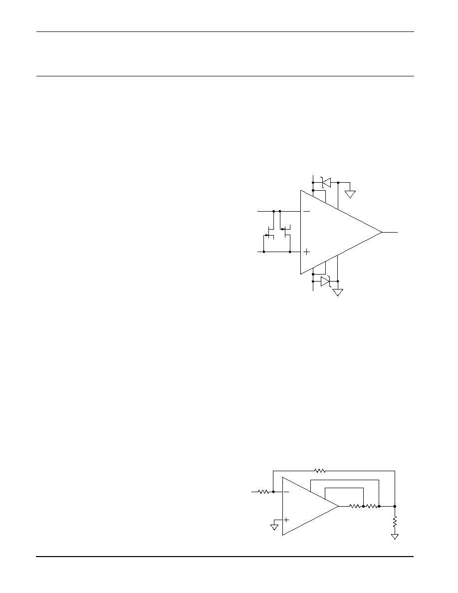
EQUIVALENT CIRCUIT DIAGRAM
42-PIN DIP
PACKAGE TYPE FC
TYPICAL APPLICATION
MOTOR POSITION CONTROL
The MOSFET output stage of the MP230 provides superior
SOA performance compared to bipolar output stages where
secondary breakdown is a concern. The extended SOA is
ideal in motor drive applications where the back EMF of the
motor may impose simultaneously both high voltage and high
current across the output stage transistors. In the figure above
a mechanical to electrical feedback position converter allows
the MP230 to drive the motor in either direction to a set point
determined by the DAC voltage.
EXTERNAL CONNECTIONS
APEX MICROTECHNOLOGY CORPORATION ∑ 5980 NORTH SHANNON ROAD ∑ TUCSON, ARIZONA 85741 ∑ USA ∑ APPLICATIONS HOTLINE: 1 (800) 546-2739
2
ABSOLUTE MAXIMUM RATINGS
SPECIFICATIONS
MP230
SPECIFICATIONS
ABSOLUTE MAXIMUM RATINGS
PARAMETER
TEST CONDITIONS
1
MIN
TYP
MAX
UNITS
INPUT
OFFSET VOLTAGE
1
5
mV
OFFSET VOLTAGE vs. temperature
Full temperature range
20
50
µV/∞C
OFFSET VOLTAGE vs. supply
20
µV/V
BIAS CURRENT, initial
3
100
pA
BIAS CURRENT vs. supply
0.1
pA/V
OFFSET CURRENT, initial
50
pA
INPUT IMPEDANCE, DC
100
G
INPUT CAPACITANCE
4
pF
COMMON MODE VOLTAGE RANGE
+V
S
- 13
V
COMMON MODE VOLTAGE RANGE
-V
S
+ 13
V
COMMON MODE REJECTION, DC
92
dB
NOISE
100kHz bandwidth, 1k R
S
5
µV RMS
SHUTDOWN, active
HSD - LSD
4.5
5
5.5
V
SHUTDOWN, inactive
HSD - LSD
-0.5
0
0.25
V
GAIN
OPEN LOOP @ 15Hz
R
L
= 1K, C
C
= 100pF
96
dB
GAIN BANDWIDTH PRODUCT @ 1MHz
C
C
= 100pF
2
MHz
PHASE MARGIN
Full temperature range
60
∞
OUTPUT
VOLTAGE SWING
I
O
= 30A
+V
S
- 10
+V
S
- 7
V
VOLTAGE SWING
I
O
= -30A
-V
S
+ 10
-V
S
+ 8
V
VOLTAGE SWING
I
O
= 30A, +V
B
= +V
S
+10V
+V
S
- 1.5
V
VOLTAGE SWING
I
O
= -30A, -V
B
= -V
S
-10V
-V
S
+ 3.0
V
CURRENT, continuous, DC
30
A
SLEW RATE, A
V
= -10
C
C
= 100pF
12
15
V/µS
SETTLING TIME, to 0.1%
A
V
= -1, 10V Step, C
C
= 470pF
2.5
µS
RESISTANCE, open loop
DC, 10A Load
0.1
POWER SUPPLY
VOLTAGE
±15
±45
±50
V
CURRENT, quiescent, total
27
35
mA
CURRENT, boost supply
17
mA
CURRENT, shutdown or class C quiescent
17
mA
THERMAL
RESISTANCE, AC, junction to case
5
Full temperature range, f 60Hz
0.6
∞C/W
RESISTANCE, DC, junction to case
Full temperature range, f < 60Hz
0.7
∞C/W
RESISTANCE, junction to air
Full temperature range
14
∞C/W
TEMPERATURE RANGE, case
-40
85
∞C
SUPPLY VOLTAGE, +V
S
to -V
S
100V
SUPPLY VOLTAGE, +V
B
(BOOST)
+V
S
+ 15V
6
SUPPLY VOLTAGE, -V
B
(BOOST)
-V
S
≠ 15V
6
OUTPUT CURRENT, peak
40A, within SOA
POWER DISSIPATION, internal, DC
210W
INPUT VOLTAGE
+V
B
to -V
B
TEMPERATURE, pin solder, 10s
225∞C.
TEMPERATURE, junction
2
175∞C.
TEMPERATURE RANGE, storage
-40 to 105∞C.
OPERATING TEMPERATURE, case
-40 to 85∞C.
NOTES: 1. Unless otherwise noted: T
C
= 25∞C, compensation C
C
= 470pF, DC input specifications are ± value given, power supply voltage
is typical rating. Amplifier operated without boost feature.
2. Long term operation at the maximum junction temperature will result in reduced product life. Derate internal power dissipation to
achieve high MTBF.
3. Doubles for every 10∞C of case temperature increase.
4. +V
S
and -V
S
denote the + and - output stage supply voltages. +V
B
and -V
B
denote the + and - input stage supply voltages (boost
voltages).
5. Rating applies if the output current alternates between both output transistors at a rate faster than 60Hz.
6. Power supply voltages +V
B
and -V
B
must not be less than +V
S
and -V
S
respectively.

APEX MICROTECHNOLOGY CORPORATION ∑ TELEPHONE (520) 690-8600 ∑ FAX (520) 888-3329 ∑ ORDERS (520) 690-8601 ∑ EMAIL prodlit@apexmicrotech.com
3
TYPICAL PERFORMANCE
GRAPHS
MP230
APEX MICROTECHNOLOGY CORPORATION ∑ 5980 NORTH SHANNON ROAD ∑ TUCSON, ARIZONA 85741 ∑ USA ∑ APPLICATIONS HOTLINE: 1 (800) 546-2739
4
OPERATING
CONSIDERATIONS
MP230
GENERAL
Please read Application Note 1 "General Operating Consid-
erations" which covers stability, power supplies, heat sinking,
mounting, current limit, SOA interpretation, and specification
interpretation. Visit www.apexmicrotech.com for design tools
that help automate tasks such as calculations for stability,
internal power dissipation, current limit, heat sink selection,
Apex's complete Application Notes library, Technical Seminar
Workbook and Evaluation Kits.
GROUND PINS
The MP230 has two ground pins (pins 2, 40). These pins
provide a return for the internal capacitive bypassing of the
small signal stages of the MP230. The two ground pins are not
connected together on the substrate. Both of these pins are
required to be connected to the system signal ground.
BALANCING RESISTOR SELECTION (R
S1
-R
S4
)
The MP230 uses parallel sets of output transistors. To ensure
that the load current is evenly shared among the transistors
external balancing resistors R
S1
-R
S4
are required. To calculate
the required value for each of the resistors use: R = 4.5 / I
2
,where I is the maximum expected output current. For example,
with a maximum output current of 10A each balancing resistor
should be 0.045 ohms. Each resistor dissipates 1.125W at the
maximum current. Use a
non-inductive 2W rated resistor. A
ready source for such resistors is the IRC resistor series LR
available from Mouser Electronics.
SAFE OPERATING AREA
The MOSFET output stage of the MP230 is not limited by
second breakdown considerations as in bipolar output stages.
Only thermal considerations and current handling capabilities
limit the SOA (see Safe Operating Area graph on previous
page). The output stage is protected against transient flyback
by the parasitic diodes of the output stage MOSFET structure.
However, for protection against sustained high energy flyback
external fast-recovery diodes must be used.
COMPENSATION
The external compensation capacitor C
C
is connected to
pins 4 and 6. Unity gain stability can be achieved with C
C
=
470pF for a minimum phase margin of 60 degrees. At higher
gains more phase shift can usually be tolerated and C
C
can be
reduced resulting in higher bandwidth and slew rate. Use the
typical operating curves as a guide to select C
C
. A 100V NPO
(COG) type capacitor is required. Boost operation requires more
compensation or higher gains than with normal operation due
to the increased capacitance of the output transistors when
the output signal swings close to the supply rails.
OVERVOLTAGE PROTECTION
Although the MP230 can withstand differential input voltages
up to ±25V, in some applications additional external protection
may be needed. 1N4148 signal diodes connected anti-parallel
across the input pins is usually sufficient. In more demanding
applications where bias current is important diode connected
JFETs such as 2N4416 will be required. See Q1 and Q2 in
Figure 1. In either case the differential input voltage will be
clamped to ±0.7V. This is sufficient overdrive to produce the
maximum power bandwidth. Some applications will also need
over-voltage protection devices connected to the power supply
rails. Unidirectional zener diode transient suppressors are
recommended. The zeners clamp transients to voltages within
the power supply rating and also clamp power supply reversals
to ground. Whether the zeners are used or not the system
power supply should be evaluated for transient performance
including power-on overshoot and power-off polarity reversals
as well as line regulation. See Z1 and Z2 in Figure 1.
POWER SUPPLY BYPASSING
Bypass capacitors to power supply terminals +V
S
and -V
S
must be connected physically close to the pins to prevent local
parasitic oscillation in the output stage of the MP230. Use
electrolytic capacitors at least 10µF per output amp required.
Bypass the electrolytic capacitors with high quality ceramic
capacitors 0.1µF or greater. In most applications power
supply terminals +V
B
and -V
B
will be connected to +V
S
and -V
S
respectively. Although +V
B
and -V
B
are bypassed internally it
is recommended to bypass +V
B
and -V
B
with 0.1µF externally.
Additionally, ground pins 2 and 40 must be connected to the
system signal ground.
CURRENT LIMIT
The two current limit sense lines are to be connected directly
across the current limit sense resistor. For the current limit to
work correctly pin 36 must be connected to the amplifier output
side and pin 35 connected to the load side of the current limit
resistor R
LIM
as shown in Figure 2. This connection will bypass

APEX MICROTECHNOLOGY CORPORATION ∑ TELEPHONE (520) 690-8600 ∑ FAX (520) 888-3329 ∑ ORDERS (520) 690-8601 ∑ EMAIL prodlit@apexmicrotech.com
5
any parasitic resistances RP, formed by socket and solder joints
as well as internal amplifi er losses.The current limiting resistor
may not be placed anywhere in the output circuit except where
shown in Figure 2. The value of the current limit resistor can
be calculated as follows: R
LIM
= .65/I
LIMIT
BOOST OPERATION
With the boost feature the small signal stages of the amplifier
are operated at a higher supply voltages than the amplifier's
high current output stage. +V
B
(pin 1) and -V
B
(pin 38) are
connected to the small signal stages. An additional 10V on the
+V
B
and -V
B
pin is sufficient to allow the small signal stages
to drive the output stage into the triode region and improve
the output voltage swing for extra efficient operation when
required. When the boost feature is not needed +V
S
and
-V
S
are connected to +V
B
and -V
B
respectively. +V
B
and -V
B
must not be operated at supply voltages less than +V
S
and
-V
S
respectively.
OPERATING
CONSIDERATIONS
MP230
SHUTDOWN
The output stage is turned off by applying a 5V level to HSD
(pin 8) relative to LSD (pin 7). This is a non-latching circuit. As
long as HSD remains high relative to LSD the output stage will
be turned off. LSD will normally be tied to signal ground but
LSD may float from -V
B
to +V
B
- 10V. Shutdown can be used
to lower quiescent current for standby operation or as part of
a load protection circuit.
BIAS CLASS OPTION
Normally pin 5 (Iq) is left open. But when pin 5 is connected
to pin 6 (Cc1) the quiescent current in the output stage is dis-
abled. This results in lower quiescent power, but also class
C operation of the output stage and the resulting crossover
distortion. In many applications, such as driving motors, the
distortion may be unimportant and lower standby power dis-
sipation is an advantage.
This data sheet has been carefully checked and is believed to be reliable, however, no responsibility is assumed for possible inaccuracies or omissions. All specifications are subject to change without notice.
MP230U REV F DECEMBER 2004 © 2004 Apex Microtechnology Corp.