 | –≠–ª–µ–∫—Ç—Ä–æ–Ω–Ω—ã–π –∫–æ–º–ø–æ–Ω–µ–Ω—Ç: MSA260 | –°–∫–∞—á–∞—Ç—å:  PDF PDF  ZIP ZIP |
APEX MICROTECHNOLOGY CORPORATION ∑ TELEPHONE (520) 690-8600 ∑ FAX (520) 888-3329 ∑ ORDERS (520) 690-8601 ∑ EMAIL prodlit@apexmicrotech.com
1
FEATURES
∑ LOW COST
∑ HIGH VOLTAGE - 450 VOLTS
∑ HIGH OUTPUT CURRENT - 20 AMPS
∑ 9kW OUTPUT CAPABILITY
∑ VARIABLE SWITCHING FREQUENCY
∑ IGBT FULL BRIDGE OUTPUT
APPLICATIONS
∑ BRUSH MOTOR CONTROL
∑ MRI
∑ MAGNETIC BEARINGS
∑ CLASS D SWITCHMODE AMPLIFIER
DESCRIPTION
The MSA260 is a surface mount constructed PWM amplifier
that provides a cost effective solution in many industrial applica-
tions. The MSA260 offers outstanding performance that rivals
many much more expensive hybrid components. The MSA260
is a complete PWM amplifier including an oscillator, comparator,
error amplifier, current limit comparators, 5V reference, a smart
controller and a full bridge IGBT output circuit. The switching
frequency is user programmable up to 50 kHz. The MSA260 is
built on a thermally conductive but electrically insulating substrate
that can be mounted to a heatsink.
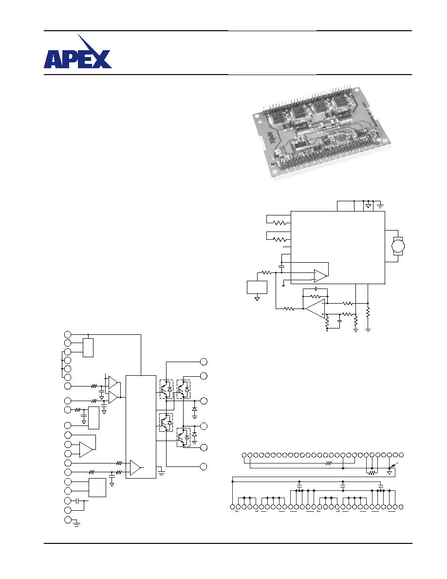
EQUIVALENT CIRCUIT DIAGRAM
58-PIN DIP
PACKAGE STYLE KC
TYPICAL APPLICATION
TORQUE MOTOR CONTROL
With the addition of a few external components the MSA260
becomes a motor torque controller. In the MSA260 the source
terminal of each low side IGBT driver is brought out for current
sensing via R
S
A and R
S
B. A1 is a differential amplifier that
amplifies the difference in currents of the two half bridges. This
signal is fed into the internal error amplifier that mixes the cur-
rent signal and the control signal. The result is an input signal
to the MSA260 that controls the torque on the motor.
EXTERNAL CONNECTIONS
VIEW FROM
COMPONENT SIDE
R
OSC
R
RAMP
+
SINGLE
POINT
GND
C3
C1
C2

APEX MICROTECHNOLOGY CORPORATION ∑ 5980 NORTH SHANNON ROAD ∑ TUCSON, ARIZONA 85741 ∑ USA ∑ APPLICATIONS HOTLINE: 1 (800) 546-2739
2
ABSOLUTE MAXIMUM RATINGS
SPECIFICATIONS
MSA260
SPECIFICATIONS
ABSOLUTE MAXIMUM RATINGS
PARAMETER
TEST CONDITIONS
1
MIN
TYP
MAX
UNITS
ERROR AMPLIFIER
OFFSET VOLTAGE
Full temperature range
9
mV
BIAS CURRENT
Full temperature range
500
nA
OFFSET CURRENT
Full temperature range
150
nA
COMMON MODE VOLTAGE RANGE
Full temperature range
0
4
V
SLEW RATE
Full temperature range
1
V/µS
OPEN LOOP GAIN
R
L
= 2K
96
dB
UNITY GAIN BANDWIDTH
1
MHz
CLOCK
LOW LEVEL OUTPUT VOLTAGE
Full temperature range
0.2
V
HIGH LEVEL OUTPUT VOLTAGE
Full temperature range
4.8
V
RISE TIME
7
nS
FALL TIME
7
nS
BIAS CURRENT, pin 22
Full temperature range
0.6
µA
5V REFERENCE OUTPUT
VOLTAGE
4.85
5.15
V
LOAD CURRENT
2
mA
OUTPUT
4
V
CE(ON)
, each active IGBT
I
CE
= 15A
2.25
V
CURRENT, continuous
V
S
= 400V, F = 22kHz
20
A
CURRENT, peak
1mS, V
S
= 400V, F = 22kHz
30
A
FLYBACK DIODE
CONTINUOUS CURRENT
20
A
FORWARD VOLTAGE
I
F
= 15A
1.5
V
REVERSE RECOVERY
I
F
= 15A
150
nS
POWER SUPPLY
VOLTAGE, V
S
5
400
450
V
VOLTAGE, V
CC
14
15
16
V
CURRENT, V
S
, quiescent
22kHz switching
9
28
mA
CURRENT, V
CC
, quiescent
22kHz switching
18
mA
CURRENT, V
CC
, shutdown
10
mA
THERMAL
RESISTANCE, DC, junction to case
Full temperature range
1
∞C/W
RESISTANCE, junction to air
Full temperature range
14
∞C/W
TEMPERATURE RANGE, case
-40
85
∞C/W
SUPPLY VOLTAGE, V
S
450V
SUPPLY VOLTAGE, V
CC
16V
OUTPUT CURRENT, peak
30A, within SOA
POWER DISSIPATION, internal, DC
250W
3
SIGNAL INPUT VOLTAGES
5.4V
TEMPERATURE, pin solder, 10s
225∞C
TEMPERATURE, junction
2
150∞C
TEMPERATURE RANGE, storage
-40∞ to 105∞C
OPERATING TEMPERATURE, case
-40∞ to 85∞C
NOTES: 1.
Unless otherwise noted: T
C
=25
∞
C, V
CC
= 15V, V
S
= 400V, F = 22kHz.
2.
Long term operation at the maximum junction temperature will result in reduced product life. Derate internal power
dissipation to achieve high MTBF.
3.
Each of the two output transistors on at any one time can dissipate 125W.
4.
Maximum specification guaranteed but not tested.

APEX MICROTECHNOLOGY CORPORATION ∑ TELEPHONE (520) 690-8600 ∑ FAX (520) 888-3329 ∑ ORDERS (520) 690-8601 ∑ EMAIL prodlit@apexmicrotech.com
3
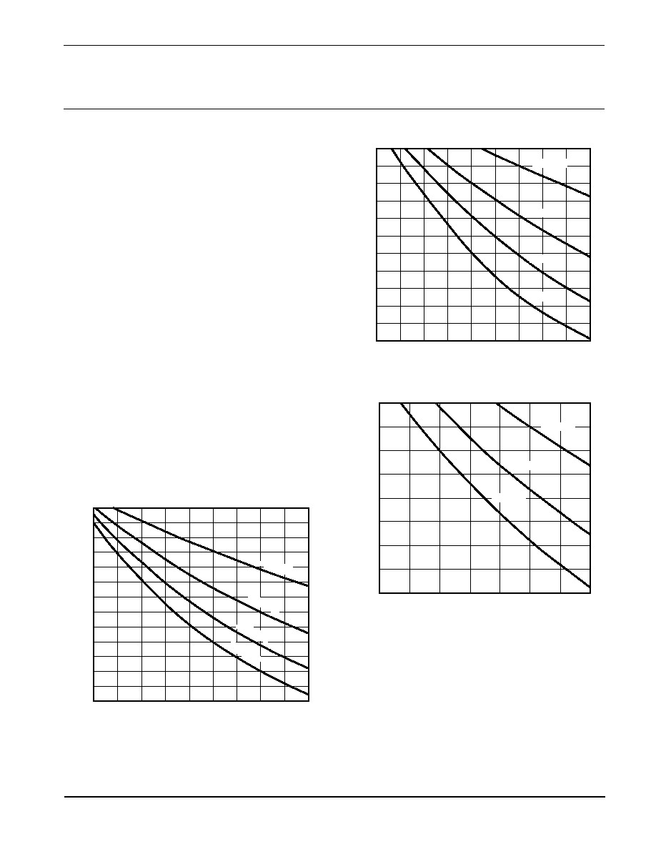
TYPICAL PERFORMANCE
GRAPHS
MSA260
APEX MICROTECHNOLOGY CORPORATION ∑ 5980 NORTH SHANNON ROAD ∑ TUCSON, ARIZONA 85741 ∑ USA ∑ APPLICATIONS HOTLINE: 1 (800) 546-2739
4
OPERATING
CONSIDERATIONS
MSA260
GENERAL
Please read Application Note 30 "PWM Basics". Refer also
to Application Note 1 "General Operating Considerations" for
helpful information regarding power supplies, heat sinking,
mounting, SOA interpretation, and specification interpreta-
tion. Visit www.apexmicrotech.com for design tools that help
automate tasks such as calculations for stability, internal power
dissipation, current limit, heat sink selection, Apex's complete
Application Notes library, Technical Seminar Workbook and
Evaluation Kits.
OSCILLATOR
The MSA260 includes a user frequency programmable
oscillator. The oscillator determines the switching frequency
of the amplifier. The switching frequency of the amplifier is
1/2 the oscillator frequency. Two resistor values must be
chosen to properly program the switching frequency of the
amplifier. One resistor, R
OSC
, sets the oscillator frequency.
The other resistor, R
RAMP
, sets the ramp amplitude. In all cases
the ramp voltage will oscillate between 1.5V and 3.5V. See
Figure 1. If an external oscillator is applied use the equations
to calculate R
RAMP
.
To program the oscillator, R
OSC
is given by:
R
OSC
= (1.32X10
8
/ F) - 2680
where F is the desired
switching frequency and:
R
RAMP
= 2 X R
OSC
Use 1% resistors with 100ppm drift (RN55C type resistors,
for example). Maximum
switching frequency is 50kHz.
Example:
If the desired
switching frequency is 22kHz then R
OSC
=
3.32K and R
RAMP
= 6.64K. Choose the closest standard 1%
values: R
OSC
= 3.32K and R
RAMP
= 6.65K or simply use two
of selected R
OSC
in series for R
RAMP
.
FIGURE 1. EXTERNAL OSCILLATOR CONNECTIONS
SHUTDOWN
The MSA260 output stage can be turned off with a shutdown
command voltage applied to Pin 10 as shown in Figure 2. The
shutdown signal is OR'ed with the current limit signal and
simply overrides it. As long as the shutdown signal remains
high the output will be off.
CURRENT SENSING
The low side drive transistors of the MSA260 are brought
out for sensing the current in each half bridge. A resistor from
each sense line to PWR GND (pin 58) develops the current
sense voltage. Choose R and C such that the time constant
is equal to 10 periods of the selected switching frequency. The
internal current limit comparators trip at 200mV. Therefore,
current limit occurs at I = 0.2/R
SENSE
for each half bridge. See
Figure 2. Accurate milliohm power resistors are required and
there are several sources for these listed in the Accessories
Vendors section of the Databook.
FIGURE 2. CURRENT LIMIT WITH OPTIONAL SHUT-
DOWN
POWER SUPPLY BYPASSING
Bypass capacitors to power supply terminals +V
S
must be
connected physically close to the pins to prevent local parasitic
oscillation and overshoot. All +V
S
must be connected together.
Place and electrolytic capacitor of at least 10µF per output amp
required midpoint between these sets of pins. In addition place
a ceramic capacitor 1.0µF or greater directly at
each set of pins
for high frequency bypassing. V
CC
is bypassed internally.
GROUNDING AND PCB LAYOUT
Switching amplifiers combine millivolt level analog signals
and large amplitude switching voltages and currents with fast
rise times. As such grounding is crucial. Use a single point
ground at SIG GND (pin 26). Connect signal ground pins 2
and 18 directly to the single point ground on pin 26. Connect
the digital return pin 23 directly to pin 26 as well. Connect
PWR GND pin 58 also to pin 26. Connect AC BACKPLATE
pin 28 also to the single point ground at pin 26. Connect the
ground terminal of the V
CC
supply directly to pin 26 as well.
Make sure no current from the load return to PWR GND flows
in the analog signal ground. Make sure that the power portion
of the PCB layout does not pass over low-level analog signal
traces on the opposite side of the PCB. Capacitive coupling
through the PCB may inject switching voltages into the analog
signal path. Further, make sure that the power side of the
PCB layout does not come close to the analog signal side.
Fast rising output signal can couple through the trace-to-trace
capacitance on the same side of the PCB.
DETERMINING THE OUTPUT STATE
The input signal is applied to +IN (Pin 13) and varies from
1.5 to 3.5 volts, zero to full scale. The ramp also varies over
the same range. When:
Ramp > +IN A
OUT
> B
OUT
The output duty cycle extremes vary somewhat with switch-
ing frequency and are internally limited to approximately 5%
to 95% at 10kHz and 7% to 93% at 50kHz.
APEX MICROTECHNOLOGY CORPORATION ∑ TELEPHONE (520) 690-8600 ∑ FAX (520) 888-3329 ∑ ORDERS (520) 690-8601 ∑ EMAIL prodlit@apexmicrotech.com
5
This data sheet has been carefully checked and is believed to be reliable, however, no responsibility is assumed for possible inaccuracies or omissions. All specifications are subject to change without notice.
MSA260U REV B JULY 2004 © 2004 Apex Microtechnology Corp.
OPERATING
CONSIDERATIONS
MSA260
CALCULATING INTERNAL POWER DISSIPATION
Detailed calculation of internal power dissipation is complex
but can be approximated with simple equations. Conduction
loss is given by:
W = I * 2.5 + I
2
* 0.095
where I = output current
Switching loss is given by:
W = 0.00046 * I * Vsupply * Fswitching
Combine these two losses to obtain total loss. Calculate
heatsink ratings and case temperatures as would be done for
a linear amplifier. For calculation of junction temperatures,
assume half the loss is dissipated in each of two switches:
Tj = Ta + Wtotal * Rÿhs + 1/2Wtotal * Rÿjc, where:
Rÿhs = heatsink rating
Rÿjc = junction-to-case thermal resistance of the
MSA260.
The SOA typical performance graphs below show perfor-
mance with the MSA260 mounted with thermal grease on the
Apex HS26. The Free Air graph assumes vertical orientation
of the heatsink and no obstruction to air flow in an ambient
temperature of 30∞C. The other two graphs show performance
with two levels of forced air. Note that air velocity is given
in linear feet per minute. As fans are rated in cubic delivery
capability, divide the cubic rating by the square area this air
flows through to find velocity. As fan delivery varies with static
pressure, these calculations are approximations, and heatsink
ratings vary with amount of power dissipated, there is no sub-
stitute for temperature measurements on the heatsink in the
center of the amplifier footprint as a final check.