 | –≠–ª–µ–∫—Ç—Ä–æ–Ω–Ω—ã–π –∫–æ–º–ø–æ–Ω–µ–Ω—Ç: PA89U | –°–∫–∞—á–∞—Ç—å:  PDF PDF  ZIP ZIP |
APEX MICROTECHNOLOGY CORPORATION ∑ TELEPHONE (520) 690-8600 ∑ FAX (520) 888-3329 ∑ ORDERS (520) 690-8601 ∑ EMAIL prodlit@apexmicrotech.com
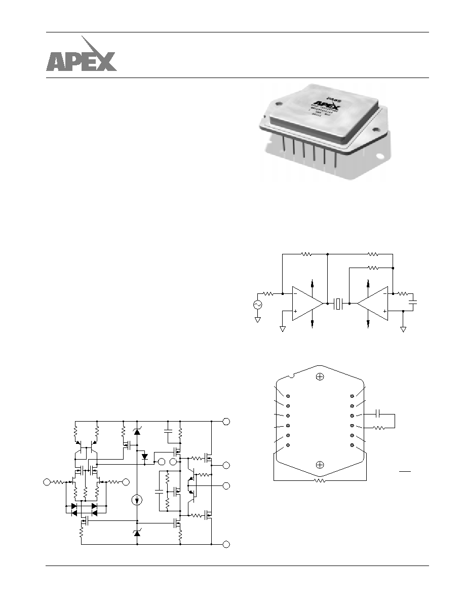
EXTERNAL CONNECTIONS*
TYPICAL APPLICATION
Ultra-high voltage capability combined with the bridge am-
plifier configuration makes it possible to develop +/≠1000 volt
peak swings across a piezo element. A high gain of ≠50 for A1
insures stability with the capacitive load, while "noise-gain"
compensation Rn and Cn on A2 insure the stability of A2 by
operating in a noise gain of 50.
A1
PA89
A2
PA89
R
50R
≠600V
V
IN
PIEZO
TRANSDUCER
50R
R
+600V
≠600V
+600V
SINGLE AXIS MICRO-POSITIONING
50R
Cn
PATENTED
PHASE COMPENSATION
Gain
C
C
R
C
1
470pF
470
10
68pF
220
15
33pF
220
100
15pF
220
Note: C
C
must be rated for full supply voltage ≠Vs to +Vs.
See details under "EXTERNAL COMPONENTS".
TOP
VIEW
≠IN
+IN
N/C
N/C
≠V
S
OUT
RESERVED
RESERVED
COMP
COMP
+V
C
S
C
C
R
C
L
R
CL
R =
CL
I
LIM
.7
1
2
3
4
5
6
12
11
10
9
8
7
TOP
VIEW
FEATURES
∑ 1140V P-P SIGNAL OUTPUT
∑ WIDE SUPPLY RANGE --
±
75V to
±
600V
∑ PROGRAMMABLE CURRENT LIMIT
∑ 75 mA CONTINUOUS OUTPUT CURRENT
∑ HERMETIC SEALED PACKAGE
∑ INPUT PROTECTION
APPLICATIONS
∑ PIEZOELECTRIC POSITIONING
∑ HIGH VOLTAGE INSTRUMENTATION
∑ ELECTROSTATIC DEFLECTION
∑ SEMICONDUCTOR TESTING
DESCRIPTION
The PA89 is an ultra high voltage, MOSFET operational
amplifier designed for output currents up to 75 mA. Output
voltages can swing over 1000V p-p. The safe operating area
(SOA) has no second breakdown limitations and can be
observed with all types of loads by choosing an appropriate
current limiting resistor. High accuracy is achieved with a
cascode input circuit configuration and 120dB open loop gain.
All internal biasing is referenced to a bootstrapped zener-
MOSFET current source, giving the PA89 a wide supply range
and excellent supply rejection. The MOSFET output stage is
biased for class A/B linear operation. External compensation
provides user flexibility. The PA89 is 100% gross leak tested
to military standards for long term reliability.
This hybrid integrated circuit utilizes a beryllia (BeO) sub-
strate, thick film resistors, ceramic capacitors and semicon-
ductor chips to maximize reliability, minimize size and give top
performance. Ultrasonically bonded aluminum wires provide
reliable interconnections at all operating temperatures. The
MO-127 High Voltage, Power DipTM package is hermetically
sealed and electrically isolated.
SIMPLIFIED SCHEMATIC
7
6
8
5
2
1
10
9
+IN
≠IN
COMP
C
OUT
+V
S
≠V
S
L
Q1
Q2
Q5
Q19
Q20
Q22
Q23
Q26
Q25A
Q25B
Q29
Q36
Q45
Q44
Q42
D1
D57
D30
D35
D34
D31
D5
H T T P : / / W W W . A P E X M I C R O T E C H . C O M ( 8 0 0 ) 5 4 6 - A P E X ( 8 0 0 ) 5 4 6 - 2 7 3 9
M I C R O T E C H N O L O G Y
HIGH VOLTAGE POWER OPERATIONAL AMPLIFIERS
PA89 ∑ PA89A
APEX MICROTECHNOLOGY CORPORATION ∑ 5980 NORTH SHANNON ROAD ∑ TUCSON, ARIZONA 85741 ∑ USA ∑ APPLICATIONS HOTLINE: 1 (800) 546-2739
ABSOLUTE MAXIMUM RATINGS
SPECIFICATIONS
PA89 ∑ PA89A
SPECIFICATIONS
ABSOLUTE MAXIMUM RATINGS
SUPPLY VOLTAGE, +V
S
to ≠V
S
1200V
OUTPUT CURRENT, within SOA
100mA
POWER DISSIPATION, internal at T
C
= 25
∞
C
40W
INPUT VOLTAGE, differential
±
25V
INPUT VOLTAGE, common mode
±
V
S
25V
TEMPERATURE, pin solder - 10s max
300
∞
C
TEMPERATURE, junction
2
150
∞
C
TEMPERATURE, storage
≠65 to 125
∞
C
OPERATING TEMPERATURE RANGE, case ≠55 to 125
∞
C
PARAMETER
TEST CONDITIONS
1
MIN
TYP
MAX
MIN
TYP
MAX
UNITS
INPUT
OFFSET VOLTAGE, initial
.5
2
.25
.5
mV
OFFSET VOLTAGE, vs. temperature
Full temperature range
10
30
5
10
µ
V/
∞
C
OFFSET VOLTAGE, vs. supply
7
*
µ
V/V
OFFSET VOLTAGE, vs. time
75
*
µ
V/kh
BIAS CURRENT, initial
3
5
50
3
10
pA
BIAS CURRENT,vs. supply
.01
*
pA/V
OFFSET CURRENT, initial
3
5
50
3
20
pA
INPUT IMPEDANCE, DC
10
5
*
M
INPUT CAPACITANCE
4
*
pF
COMMON MODE VOLTAGE RANGE
4
Full temperature range
±
V
S
50
*
V
COMMON MODE REJECTION, DC
Full temperature range, V
CM
=
±
90V
96
110
*
*
dB
INPUT NOISE
10kHz BW, R
S
= 10K, C
C
= 15pF
4
µ
V RMS
GAIN
OPEN LOOP GAIN at 10Hz
R
L
= 10k, C
C
= 15pF
108
120
*
*
dB
GAIN BANDWIDTH PRODUCT
R
L
= 10k, C
C
= 15pF, A
V
= 100
10
*
MHz
POWER BANDWIDTH
R
L
= 10k, C
C
= 15pF, V
O
= 500V p-p
5
*
kHz
PHASE MARGIN
Full temperature range, A
V
= 10
60
*
∞
OUTPUT
VOLTAGE SWING
4
I
O
= 75mA
±
V
S
30
±
V
S
15
*
*
V
VOLTAGE SWING
4
Full temperature range, I
O
= 20mA
±
V
S
20
±
V
S
12
*
*
V
CURRENT, continuous
Full temperature range
75
*
mA
SLEW RATE
C
C
= 15pF, A
V
= 100
12
16
*
*
V/
µ
s
CAPACITIVE LOAD, Av = 10
Full temperature range
1
*
nF
CAPACITIVE LOAD, Av>10
Full temperature range
SOA
*
SETTLING TIME to .1%
R
L
= 10K
, 10V step, Av = 10
2
*
µ
s
POWER SUPPLY
VOLTAGE, V
S
4
Full temperature range
±
75
±
500
±
600
*
*
*
V
CURRENT, quiescent
4.8
6.0
*
*
mA
THERMAL
RESISTANCE, AC, junction to case
5
Full temperature range, F > 60Hz
2.1
2.3
*
*
∞
C/W
RESISTANCE, DC, junction to case
Full temperature range, F < 60Hz
3.3
3.5
*
*
∞
C/W
RESISTANCE, junction to air
Full temperature range
15
*
∞
C/W
TEMPERATURE RANGE, case
Meets full range specifications
≠25
+85
*
*
∞
C
PA89A
PA89
±
NOTES:
*
The specification of PA89A is identical to the specification for PA89 in applicable column to the left.
1.
Unless otherwise noted: T
C
= 25
∞
C, C
C
= 68pF, R
C
= 220
, and V
S
=
±
500V. Input parameters for bias currents and offset
voltage are
±
values given.
2.
Long term operation at the maximum junction temperature will result in reduced product life. Derate internal power dissipation
to achieve high MTTF.
3.
Doubles for every 10
∞
C of temperature increase.
4.
+V
S
and ≠V
S
denote the positive and negative supply rail respectively.
5.
Rating applies only if the output current alternates between both output transistors at a rate faster than 60Hz.
The PA89 is constructed from MOSFET transistors. ESD handling procedures must be observed.
The internal substrate contains beryllia (BeO). Do not break the seal. If accidentally broken, do not crush, machine, or
subject to temperatures in excess of 850
∞
C to avoid generating toxic fumes.
CAUTION
±
±
±
±
±
APEX MICROTECHNOLOGY CORPORATION ∑ TELEPHONE (520) 690-8600 ∑ FAX (520) 888-3329 ∑ ORDERS (520) 690-8601 ∑ EMAIL prodlit@apexmicrotech.com
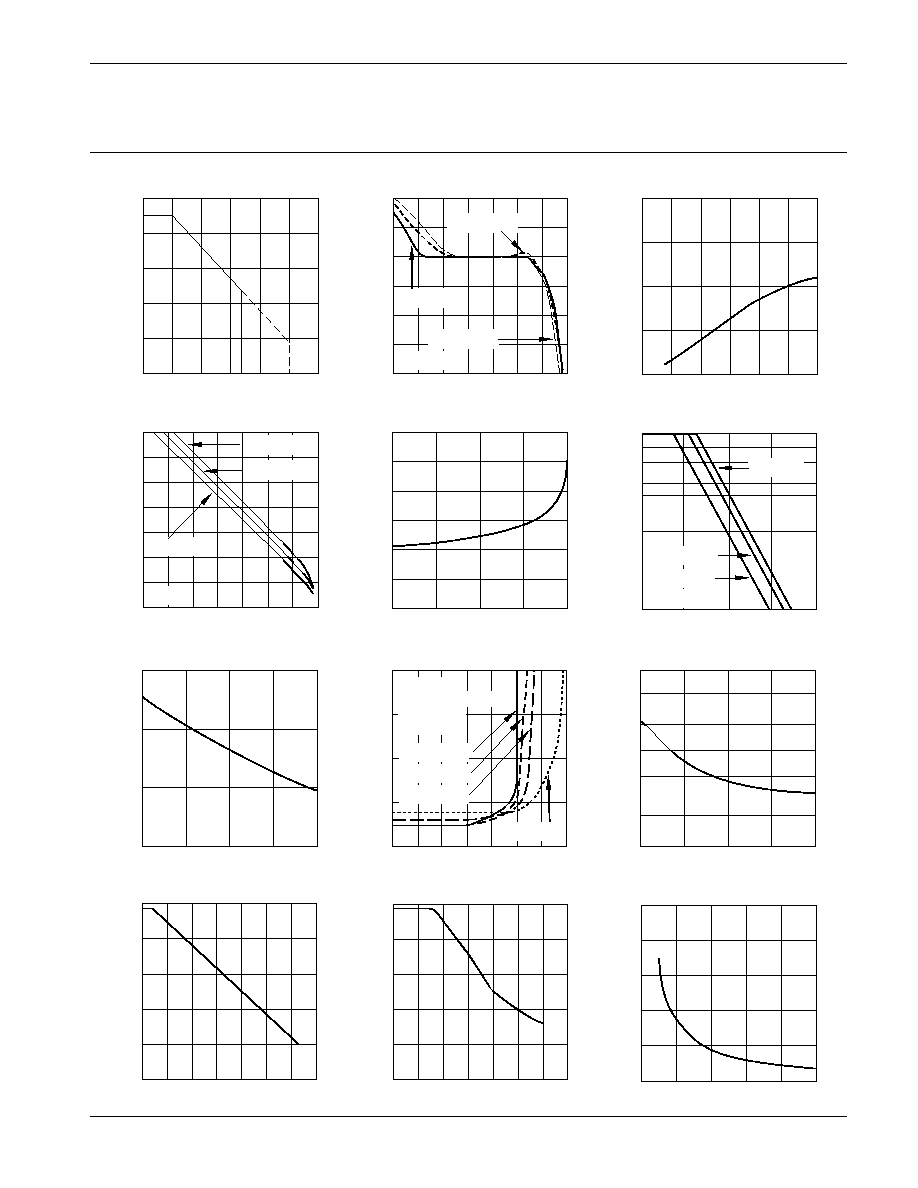
TYPICAL PERFORMANCE
GRAPHS
PA89 ∑ PA89A
0
25
50
75
100
125
150
CASE TEMPERATURE, T (∞C)
0
8
24
32
POWER DERATING
OUTPUT STAGE
INTERNAL POWER DISSIPATION, P(W)
1
100
1K
10M
FREQUENCY F (Hz)
≠270
≠180
≠45
0
PHASE RESPONSE
PHASE, (∞)
≠135
≠225
10
100
10K
100K
FREQUENCY, F (Hz)
INPUT NOISE VOLTAGE, e (nV/ Hz)
1
100
10M
FREQUENCY, F (Hz)
≠20
0
60
120
SMALL SIGNAL RESPONSE
OPEN LOOP GAIN, A (dB)
20
40
80
100
0
25
75
100
OUTPUT CURRENT, I (mA)
5
10
20
30
OUTPUT VOLTAGE SWING
15
25
1K
3K
30K
100K
FREQUENCY, F (Hz)
100
500
1000
OUTPUT VOLTAGE, V (V )
O
300
600
1
100
10K
10M
FREQUENCY, F (Hz)
0
60
100
COMMON MODE REJECTION
COMMON MODE REJECTION, CMR(dB)
20
40
80
1
10M
FREQUENCY, F (Hz)
0
20
100
POWER SUPPLY REJECTION
POWER SUPPLY REJECTION, PSR (dB)
40
80
0
40
60
100
RESISTOR VALUE, R ( )
0
40
100
CURRENT LIMIT
CURRENT LIMIT, I (mA)
LIM
60
80
0
75
EXT. COMPENSATION CAPACITOR, C (pF)
5
SLEW RATE VS COMP
SLEW RATE, (V/ S)
10
15
20
100
25
50.
30
300
3K
FREQUENCY, F (Hz)
.01
.1
HARMONIC DISTORTION
DISTORTION, THD(%)
1
10
100K
100
1K
10K
0
200
800
1200
TOTAL SUPPLY VOLTAGE, V (V)
.9
1.10
QUIESCENT CURRENT
NORMALIZED QUIESCENT CURRENT, I (X)
Q
1.05
S
10
1K
100K 1M
CL
20
80
20
30K
S
C
L
INPUT NOISE VOLTAGE
1K
2
7
10
20
3
5
15
N
O
50
VOLTAGE DROP FROM SUPPLY, V ≠ V (V)
SO
15pf, 220
33pf, 220
68pf, 220
10
10K 100K 1M
≠90
16
40
POWER RESPONSE
800
1200
PP
10K
C = 68pf
C
C = 33pf
C
C = 15pf
C
10 100 1K 10K 100K 1M
60
400
600
1000
.95
1.00
µ
C
68pf, 220
33pf, 220
15pf, 220
V = 800Vpp
O
V = 600Vpp
O
V = 400Vpp
O
V = 100Vpp
O
.001
10
1K
10K 100K 1M
C , R
C
C
C , R
C
C
R = 220
C
V = ±500V
C = 15pf,
R = 11K
A = 100
R = 220
C
V
APEX MICROTECHNOLOGY CORPORATION ∑ 5980 NORTH SHANNON ROAD ∑ TUCSON, ARIZONA 85741 ∑ USA ∑ APPLICATIONS HOTLINE: 1 (800) 546-2739
OPERATING
CONSIDERATIONS
PA89 ∑ PA89A
GENERAL
Please read the "General Operating Considerations" sec-
tion, which covers stability, supplies, heatsinking, mounting,
current limit, SOA interpretation, and specification interpreta-
tion. Additional information can be found in the application
notes. For information on the package outline, heatsinks, and
mounting hardware, consult the "Accessory and Package
Mechanical Data" section of the handbook.
STABILITY
Although the PA89 can be operated at unity gain, maximum
slew rate and bandwidth performance was designed to be
obtained at gains of 10 or more. Use the small signal response
and phase response graphs as a guide. In applications where
gains of less than 10 are required, use noise gain compensa-
tion to increase the phase margin of the application circuit as
illustrated in the typical application drawing.
SAFE OPERATING AREA (SOA)
The MOSFET output stage of this power operational ampli-
fier has two distinct limitations:
1.
The current handling capability of the MOSFET geometry
and the wire bonds.
2.
The junction temperature of the output MOSFETs.
NOTE: The output stage is protected against transient flyback.
However, for protection against sustained, high energy flyback,
external fast-recovery diodes should be used.
SAFE OPERATING CURVES
The safe operating area curves define the maximum addi-
tional internal power dissipation the amplifier can tolerate when
it produces the necessary output to drive an external load. This
is not the same as the absolute maximum internal power
dissipation listed elsewhere in the specification since the quies-
cent power dissipation is significant compared to the total.
EXTERNAL COMPONENTS
The very high operating voltages of the PA89 demand
consideration of two component specifications rarely of con-
cern in building op amp circuits: voltage rating and voltage
coefficient.
The compensation capacitance C
C
must be rated for the full
supply voltage range. For example, with supply voltages of
±
500V the possible voltage swing across C
C
is 1000V. In
addition, a voltage coefficient less than 100PPM is recom-
mended to maintain the capacitance variation to less than 5%
for this example. It is strongly recommended to use the highest
quality capacitor possible rated at least twice the total supply
voltage range.
Of equal importance are the voltage rating and voltage
coefficient of the gain setting resistances. Typical voltage
ratings of low wattage resistors are 150 to 250V. In the above
example 1000V could appear across the feedback resistor.
This would require several resistors in series to obtain the
proper voltage rating. Low voltage coefficient resistors will
insure good gain linearity. The wattage rating of the feedback
resistor is also of concern. A 1 megohm feedback resistor
could easily develop 1 watt of power dissipation.
Though high voltage rated resistors can be obtained,
a 1 megohm feedback resistor comprised of five 200Kohm, 1/
4 watt metal film resistors in series will produce the proper
voltage rating, voltage coefficient and wattage rating.
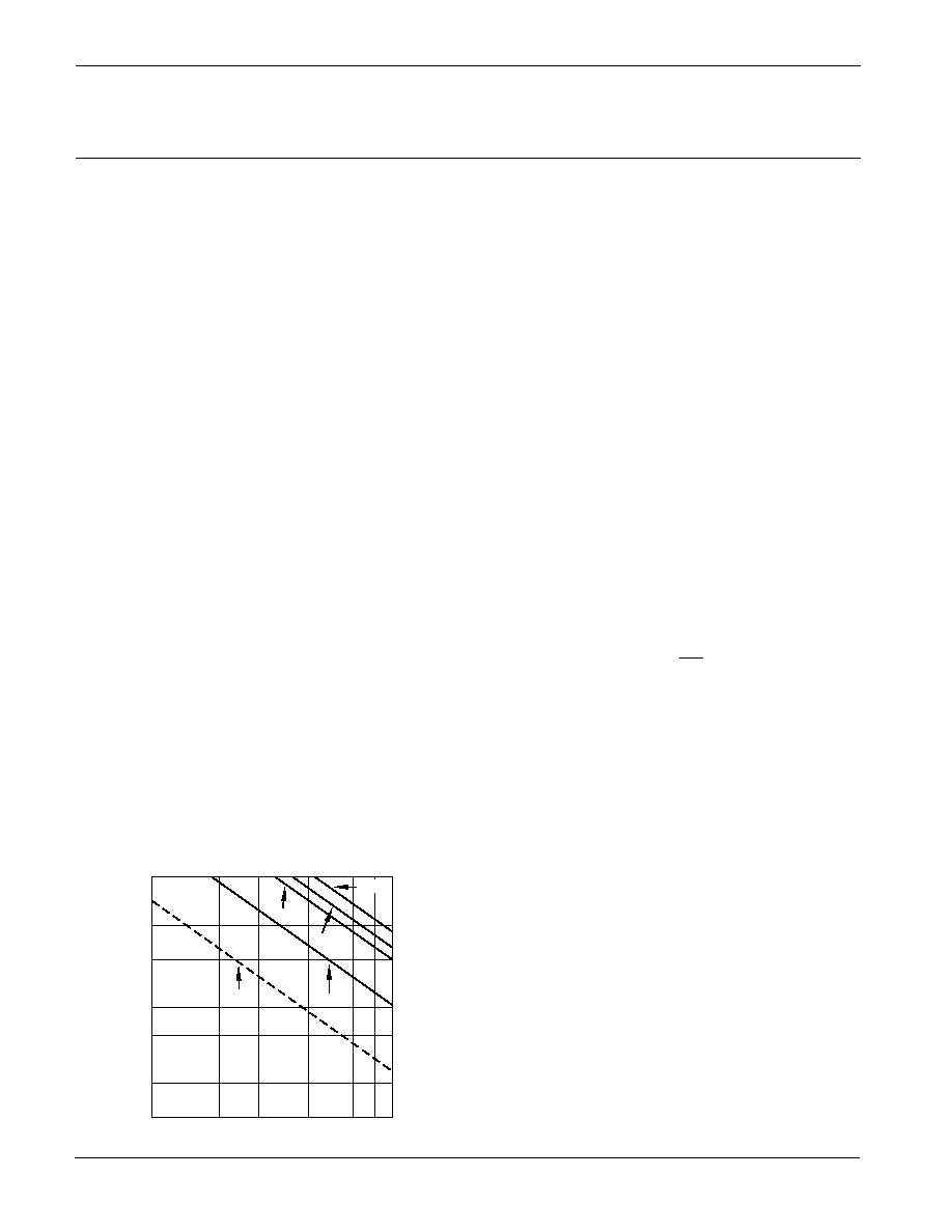
CURRENT LIMIT
For proper operation the current limit resistor (R
CL
) must be
connected as shown in the external connection diagram. The
minimum value is 3.5 ohm, however for optimum reliability the
resistor value should be set as high as possible. The value is
calculated as follows with the maximum practical value of 150
ohms.
R
CL
=
When setting the value for R
CL
allow for the load current as
well as the current in the feedback resistor. Also allow for the
temperature coefficient of the current limit which is approxi-
mately -0.3% /
∞
C of case temperature rise.
CAUTIONS
The operating voltages of the PA89 are potentially lethal.
During circuit design, develop a functioning circuit at the lowest
possible voltages. Clip test leads should be used for "hands
off" measurements while troubleshooting.
POWER SUPPLY PROTECTION
Unidirectional zener diode transient absorbers are recom-
mended as protection on the supply pins. The zeners clamp
transients to voltages within the power supply rating and also
clamp power supply reversals to ground. Whether the zeners
are used or not, the system power supply should be evaluated
for transient performance including power-on overshoot and
power-off polarity reversals as well as line regulation.
Conditions which can cause open circuits or polarity rever-
sals on either power supply rail should be avoided or protected
against. Reversals or opens on the negative supply rail is
known to induce input stage failure. Unidirectional transzorbs
prevent this, and it is desirable that they be both electrically and
physically as close to the amplifier as possible.
.7
I
LIM
100
300
500
800 1000 1200
SUPPLY TO OUTPUT DIFFERENTIAL VOLTAGE, V ≠ V (V)
S
O
3
10
30
OUTPUT CURRENT FROM +V OR ≠V (mA)
SS
100
200
5
15
50
100mS
25∞C
85∞C
125∞C
T = T
CASE
10mS
This data sheet has been carefully checked and is believed to be reliable, however, no responsibility is assumed for possible inaccuracies or omissions. All specifications are subject to change without notice.
PA89U REV. F FEBRUARY 1998
© 1998 Apex Microtechnology Corp.