 | –≠–ª–µ–∫—Ç—Ä–æ–Ω–Ω—ã–π –∫–æ–º–ø–æ–Ω–µ–Ω—Ç: PA96 | –°–∫–∞—á–∞—Ç—å:  PDF PDF  ZIP ZIP |
APEX MICROTECHNOLOGY CORPORATION ∑ TELEPHONE (520) 690-8600 ∑ FAX (520) 888-3329 ∑ ORDERS (520) 690-8601 ∑ EMAIL prodlit@apexmicrotech.com
1
D
P
A96
FEATURES
∑ HIGH VOLTAGE - 300 VOLTS
∑ HIGH OUTPUT CURRENT ≠ 1.5 AMPS
∑ 70 WATT DISSIPATION CAPABILITY
∑ 175 MHz GAIN BANDWIDTH
∑ 250 V/µ-SECOND SLEW RATE
APPLICATIONS
∑ PZT DRIVE
∑ MAGNETIC DEFLECTION
∑ PROGRAMMABLE POWER SUPPLIES
∑ 70V LINE AUDIO to 70W
DESCRIPTION
The PA96 is a state of the art high voltage, high current
operational amplifier designed to drive resistive, capacitive
and inductive loads. For optimum linearity, the output stage
is biased for class A/B operation. External compensation
provides user flexibility in maximizing bandwidth at any gain
setting. The safe operating area (SOA) can be observed for
all operating conditions by selection of user programmable
current limit. For continuous operation under load, a heatsink
of proper rating is required.
The hybrid integrated circuit utilizes thick film (cermet)
resistors, ceramic capacitors and semiconductor chips to
maximize reliability, minimize size and give top performance.
Ultrasonically bonded aluminum wires provide reliable inter-
connections at all operating temperatures. The 8-pin TO-3
package is hermetically sealed and electrically isolated. The
use of compressible isolation washers voids the warranty.
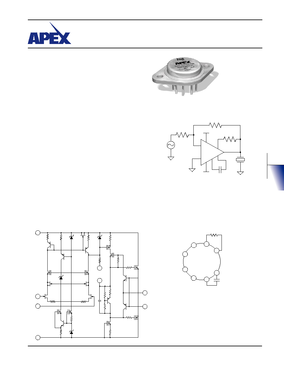
EQUIVALENT CIRCUIT DIAGRAM
TYPICAL APPLICATION
PZT POSITION CONTROL
The MOSFET output stage of the PA96 provides superior
SOA performance compared to bipolar output stages where
secondary breakdown is a concern. The extended SOA is
ideal in applications where the load is highly reactive and
may impose simultaneously both high voltage and high cur-
rent across the output stage transistors. In the figure above
a piezo-electric transducer is driven to high currents and high
voltages by the PA96.
EXTERNAL CONNECTIONS
8-PIN TO-3
PACKAGE STYLE CE

APEX MICROTECHNOLOGY CORPORATION ∑ 5980 NORTH SHANNON ROAD ∑ TUCSON, ARIZONA 85741 ∑ USA ∑ APPLICATIONS HOTLINE: 1 (800) 546-2739
2
ABSOLUTE MAXIMUM RATINGS
SPECIFICATIONS
SPECIFICATIONS
ABSOLUTE MAXIMUM RATINGS
SUPPLY VOLTAGE, +V
S
to -V
S
300V
OUTPUT CURRENT, continuous
1.5A,
POWER DISSIPATION, internal, DC
70W
INPUT VOLTAGE, common mode
+V
S
to -V
S
INPUT VOLTAGE, differential
±15V
TEMPERATURE, pin solder, 10s
300∞C
TEMPERATURE, junction
2
150∞C
TEMPERATURE RANGE, storage
-65 to 150∞C
OPERATING TEMPERATURE, case
-55 to 125∞C
PARAMETER
TEST CONDITIONS1
MIN
TYP
MAX
UNITS
INPUT
OFFSET VOLTAGE
1
5
mV
OFFSET VOLTAGE vs. temperature
Full temperature range
20
50
µV/∞C
OFFSET VOLTAGE vs. supply
20
µV/V
BIAS CURRENT, initial
3
200
pA
BIAS CURRENT vs. supply
0.1
pA/V
OFFSET CURRENT, initial
50
pA
INPUT RESISTANCE, DC
100
G
INPUT CAPACITANCE
4
pF
COMMON MODE VOLTAGE RANGE
+V
S
- 13
V
COMMON MODE VOLTAGE RANGE
-V
S
+ 13
V
COMMON MODE REJECTION, DC
92
dB
NOISE
100KHz bandwidth, 1k R
s
6
µV RMS
GAIN
OPEN LOOP @ 15Hz
R
L
= 1k, C
C
=100pF
96
114
dB
GAIN BANDWIDTH PRODUCT @ 1MHz VS = 150V, -VS = 150V,
100
175
MHz
A = -100, RF = 100K
PHASE MARGIN
Full temperature range, using
60
∞
recommended C
C
for gain.
PBW
250V p-p output, 100,
100
KHz
+150V Supplies, Cc = 0pf
OUTPUT
VOLTAGE SWING
I
O
= 1.5A
+V
S
- 12
+V
S
- 5.6
V
VOLTAGE SWING
I
O
= -1.5A
-V
S
+ 12
-V
S
+ 10
V
VOLTAGE SWING
I
O
= 0.1A
+V
S
- 8
V
VOLTAGE SWING
I
O
= -0.1A
-V
S
+ 8
V
CURRENT, continuous, DC
1.5
A
SLEW RATE
A
V
= -100, ±150V Supplies, 250 load
200
250
V/µS
negative slope, Positiveslope much
faster
SETTLING TIME, to 0.1%
A
V
= -100, 1V Step, C
C
= 0pF
2
µS
RESISTANCE, open loop
DC, 1A Load
7
10
THERMAL
RESISTANCE, AC Junction to Case
Full temperature range. f > 60Hz
1.2
1.3
∞C/W
RESISTANCE, DC Junction to Case
Full temperature range. f < 60Hz
1.6
1.8
∞C/W
RESISTANCE, Junction to Ambient
30
∞C/W
POWER SUPPLY
VOLTAGE
±15
±100
±150
V
CURRENT, Quiescent total
25
30
35
mA
CURRENT, Quiescent output stage only
10
mA
PA96
NOTES: * The specification of PA08A is identical to the specification for PA08 in applicable column to the left.
1. Long term operation at the maximum junction temperature will result in reduced product life. Derate power dissipation to achieve
high MTTF.
2. The power supply voltage specified under typical (TYP) applies unless otherwise noted.
3. Doubles for every 10
o
C of temperature increase.
4. +V
S
and ≠V
S
denote the positive and negative supply rail respectively.
5. Rating applies only if output current alternates between both output transistors at a rate faster than 60Hz.
The internal substrate contains beryllia (BeO). Do not break the seal. If accidentally broken, do not crush, machine, or
subject to temperatures in excess of 850∞C to avoid generating toxic fumes.
CAUTION

APEX MICROTECHNOLOGY CORPORATION ∑ TELEPHONE (520) 690-8600 ∑ FAX (520) 888-3329 ∑ ORDERS (520) 690-8601 ∑ EMAIL prodlit@apexmicrotech.com
3
D
P
A96
TYPICAL PERFORMANCE
GRAPHS
PA96

APEX MICROTECHNOLOGY CORPORATION ∑ 5980 NORTH SHANNON ROAD ∑ TUCSON, ARIZONA 85741 ∑ USA ∑ APPLICATIONS HOTLINE: 1 (800) 546-2739
4
OPERATING
CONSIDERATIONS
PA96
GENERAL
Please read Application Note 1 "General Operating Con-
siderations" which covers stability, supplies, heat sinking,
mounting, current limit, SOA interpretation, and specification
interpretation. Visit www.apexmicrotech.com for design tools
that help automate tasks such as calculations for stability,
internal power dissipation, current limit, heat sink selection,
Apex's Application Notes library, Technical Seminar Workbook,
and Evaluation Kits.
SPECIAL PRECAUTIONS
The PA96 operates with up 300V rail to rail voltage, and
delivers amperes of current. Precautions should be taken for
the safety of the user and the amplifier.
Although the non-operating common mode input range is rail
to rail, the differential input voltage must not exceed ±15 V.
Therefore; if the feedback ratio is less than 10, even if
caused by disconnecting a signal source , typical power turn
on transients can destroy the amplifier.
Similarly in a voltage follower application a large differential
transient can be generated if the slew rate of the input is greater
than that of the voltage follower.
Therefore it is prudent to clamp the input with series back
to back diodes as shown below.
If experimentally optimizing the compensation capacitor,
turn off the supplies and let them bleed to low voltage before
installing each new value. Otherwise internal current pulses of
up to 3 amps can be induced. Also, do you want your fingers
around 300V?
Essentially the full rail to rail power supply voltage may be
applied to the compensation capacitor. A 400V COG or Mica
capacitor is recommended.
POWER BANDWIDTH
The power bandwidth is 1/( x the negative edge slew time).
The slew time is determined by the compensation capacitor,
load, and internal device capacitance; it is independent of
closed loop gain. The uncompensated power bandwidth is
typically 100kHz for a 250Vp-p output signal into 100
. It typi-
cally increases to above 300KHz with no load.
COMPENSATION TABLE
The following table tabulates recommended compensation
capacitor values vs. gain. These values will typically result in
less than 2% overshoot and a -3db small signal bandwidth of
greater than 1MHz, except under operating conditions where
uncompensated gain bandwidth is too low to support a 1MHz
bandwidth. (See gain bandwidth vs. Plus power supply curves).
Note that other factors such as capacitance in parallel with
the feedback resistor may reduce circuit bandwidth from that
determined from the gain bandwidth curve.
Cc
Inverting Gain
From
To
150pf
1
2
51pf
2
5
33pf
5
10
22pf
10
20
10pf
20
50
5pf
50
100
None
100
up
Cc
Non-Inverting Gain
From
To
330 pf
1
2
150pf
2
3
51pf
3
6
33pf
6
10
22pf
10
20
10pf
20
50
5pf
50
100
None
100
up
CURRENT LIMIT
For proper operation the current limit resistor, Rcl, must
be connected as shown in the external connections diagram.
The minimum value is 0.2, with a maximum practical value of
100. For optimum reliability the resistor should be set as high
as possible. The value is calculated as I
L
= 0.68V/Rcl. Note that
the 0.68V is reduced by 2mV every ∞C rise in temperature.
Also note that the current limit can be set such that the SOA
is exceeded on a continuous basis. As an example if the current
limit was set at 1.5A and the supply was at 150V, a short to
ground would produce 225 watts internal dissipation, greatly
exceeding the 83 watt steady state SOA rating.
Under some conditions of load and compensation the am-
plifier may oscillate at a low level when current limit is active,
even though the amplifier is stable otherwise. The current
will be limited to the programmed value in this situation. To
minimize such occurrences, use a non-reactive resistor to
program current limit.
This data sheet has been carefully checked and is believed to be reliable, however, no responsibility is assumed for possible inaccuracies or omissions. All specifications are subject to change without notice.
PA96U REV B DECEMBER 2005 © 2005 Apex Microtechnology Corp.