 | –≠–ª–µ–∫—Ç—Ä–æ–Ω–Ω—ã–π –∫–æ–º–ø–æ–Ω–µ–Ω—Ç: SA07U | –°–∫–∞—á–∞—Ç—å:  PDF PDF  ZIP ZIP |

APEX MICROTECHNOLOGY CORPORATION ∑ TELEPHONE (520) 690-8600 ∑ FAX (520) 888-3329 ∑ ORDERS (520) 690-8601 ∑ EMAIL prodlit@apexmicrotech.com
MB
3 0
9
Q
9 3
1 7
U S
A
B e
O
6 0
0 2
4
SA07
FEATURES
∑ 500kHz SWITCHING
∑ FULL BRIDGE OUTPUT 5-40V (80V P-P)
∑ 5A OUTPUT
∑ 1 IN
2
FOOTPRINT
∑ FAULT PROTECTION
∑ SHUTDOWN CONTROL
∑ SYNCHRONIZABLE CLOCK
∑ HERMETIC PACKAGE
APPLICATIONS
∑ HIGH FIDELITY AUDIO AMPLIFIER
∑ BRUSH TYPE MOTOR CONTROL
∑ VIBRATION CANCELLING AMPLIFIER
DESCRIPTION
The SA07 amplifier is a 40 volt, 500kHz PWM amplifier. The
full bridge output circuit provides 5 amps of continuous drive
current for applications as diverse as high fidelity audio and
brush type motors. Clock output and input pins can be used for
synchronization with other amplifiers or an externally gener-
ated clock. An integrator amplifier is provided. Direct access
to the pwm input is provided for connection to digital motion
control circuits. Protection circuits guard against thermal over-
loads as well as shorts to supply or ground. The current limit
is programmable with one or two external resistors depending
on the application. A shutdown input disables all output bridge
drivers. The 18 pin steel package is hermetically sealed.
BLOCK DIAGRAM AND
TYPICAL APPLICATION
CONNECTIONS
HIGH FIDELITY
AUDIO
EXTERNAL CONNECTIONS
Case tied to Pin 7. Allow no current in case. Bypassing of supplies is
required. Package is Apex DIP6. See Outline Dimensions/Packages. If
+PWM > RAMP then A OUT > B OUT.
* See text.
18
17
16
15
14
13
12
11
10
Isense B
B OUT
+Vs
A OUT
Isense A
Vcc
Rlimit*
Rlimit*
*
*
CLK OUT*
CLK IN
Ilim/SHDN
1
2
3
4
5
6
7
8
9
5V OUT
≠INT
+INT
INT OUT*
+PWM
RAMP/≠PWM
GND
NC
NC
B
R
I
D
G
E
D
R
I
V
E
R
THERMAL,
SHORT
CIRCUIT
PROTECT.
REG.
5V
+V
S
A OUT
5V OUT
B OUT
ILIM/SHDN
I SENSE A
I SENSE B
+PWM
RAMP/≠PWM
CLK OUT
18K
100pF
CLK IN
INT OUT
INT ≠
OSC
CLK/2
R
FILTER
C
FILTER
R
SHDN
1K
R
LIMIT
SIGNAL
GND
5V
LOAD
SA07
INT +
Vcc
13
10
12
14
16
11
15
1
5
6
18
17
7
4
3
2
H T T P : / / W W W . A P E X M I C R O T E C H . C O M ( 8 0 0 ) 5 4 6 - A P E X ( 8 0 0 ) 5 4 6 - 2 7 3 9
M I C R O T E C H N O L O G Y
PULSE WIDTH MODULATION AMPLIFIER
SA07
APEX MICROTECHNOLOGY CORPORATION ∑ 5980 NORTH SHANNON ROAD ∑ TUCSON, ARIZONA 85741 ∑ USA ∑ APPLICATIONS HOTLINE: 1 (800) 546-2739
ABSOLUTE MAXIMUM RATINGS
SPECIFICATIONS
ABSOLUTE MAXIMUM RATINGS
SUPPLY VOLTAGE, +V
S
to GND, 10mS surge 60V
SUPPLY VOLTAGE, V
CC
to GND
16V
OUTPUT CURRENT, peak
7.5A
POWER DISSIPATION, internal
80W
1
TEMPERATURE, pin solder - 10s
300
∞
C
TEMPERATURE, junction
2
150
∞
C
TEMPERATURE, storage
≠65 to +150
∞
C
OPERATING TEMPERATURE RANGE, case
≠55 to +125
∞
C
INPUTS
≠.4/+5.4V
SA07
The SA07 is constructed from MOSFET transistors. ESD handling procedures must be observed.
The internal substrate contains beryllia (BeO). Do not break the seal. If accidentally broken, do not crush, machine, or
subject to temperatures in excess of 850
∞
C to avoid generating toxic fumes.
CAUTION
NOTES: 1.
40W in each of the two active output transistors on at any one time.
2.
Unless otherwise noted: T
C
= 25
∞
C.
3.
Min max values guaranteed but not tested.
4.
Long term operation at the maximum junction temperature will result in reduced product life. Derate internal power dissipation
to achieve high MTTF. For guidance, refer to the heatsink data sheet.
SPECIFICATIONS
PARAMETER
TEST CONDITIONS
2
MIN
TYP
MAX
UNITS
ERROR AMP, CLOCK REF
3
OFFSET VOLTAGE
10
mV
BIAS CURRENT
50
pA
OFFSET CURRENT
30
pA
COMMON MODE VOLTAGE RANGE
0
3
V
COMMON MODE REJECTION, DC
70
dB
SLEW RATE
12
V/
µ
S
OPEN LOOP GAIN
100
dB
GAIN BANDWIDTH PRODUCT
10
MHz
CLOCK OUT
.98
1
1.02
MHz
CLOCK OUT, high level
4.7
5.3
V
CLOCK OUT, low level
0
.2
V
5V OUT
LOAD
5mA
4.988
5
5.012
V
OUTPUT
EFFICIENCY, 5A output
V
S
= 40V
94
%
SWITCHING FREQUENCY
500
kHz
CURRENT, continuous
5
A
CURRENT, peak
3
100 ms, 10% duty cycle
7
A
R
DS(ON)
3
.55
POWER SUPPLY
VOLTAGE, V
CC
Full temperature range
10
12
16
V
VOLTAGE, V
S
Full temperature range
5
40
V
CURRENT, V
CC
Switching
50
mA
CURRENT, V
S
Switching, No Load
90
mA
INPUTS
3
I
LIM
/SHDN, trip point
90
110
mV
≠PWM, +PWM, low level
0
.8
V
≠PWM, +PWM, high level
2.7
Vcc
V
CLOCK IN, low level
0
.3
V
CLOCK IN, high level
3
5.6
V
THERMAL
4
RESISTANCE, junction to case
Full temperature range
3.5
∞
C/W
RESISTANCE, junction to air
Full temperature range
15
∞
C/W
TEMPERATURE RANGE, case
Meets full range specifications
≠25
85
∞
C
APEX MICROTECHNOLOGY CORPORATION ∑ TELEPHONE (520) 690-8600 ∑ FAX (520) 888-3329 ∑ ORDERS (520) 690-8601 ∑ EMAIL prodlit@apexmicrotech.com
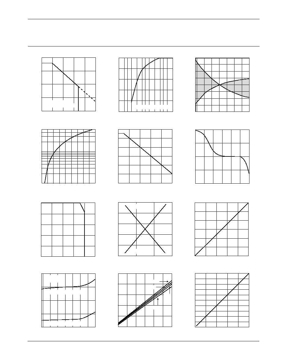
OPERATING
CONSIDERATIONS
SA07
0
100
200
300
400
500
40
50
60
70
80
90
100
Vcc QUIESCENT CURRENT
NORMALIZED Vcc QUIESCENT CURRENT, (%)
100
97.5
99.0
99.5
100
CLOCK LOADING
98.0
98.5
1K
10K
NORMALIZED FREQUENCY, (%)
SWITCHING FREQUENCY, F (kHz)
CLOCK LOAD RESISTANCE, (
)
0.6
1.8
2.2 2.4
SOURCE TO DRAIN DIODE VOLTAGE
5
REVERSE DIODE
FLYBACK CURRENT, Isd (A)
2
3
4
1.0
2
3
4
5
25
50
75
100
125
150
3
4
5
CONTINUOUS OUTPUT
2
FREQUENCY, F (Hz)
≠180
INTEGRATOR PHASE
1.0
1.4
≠50
10
15
20
25
30
35
40
125
≠25
0
25
50
75 100
10
100
1K
10K 100K 1M
10M
CASE TEMPERATURE, (
∞
C)
CONTINUOUS AMPS
≠135
≠90
≠45
0
OPEN LOOP PHASE,
(
∞
)
0
1
0
75
100
CASE TEMPERATURE, (
∞
C)
0
POWER DERATING
40
25
DUTY CYCLE VS ANALOG INPUT
DUTY CYCLE, (%)
50
125
10
20
30
0
20
40
60
80
100
INTERNAL POWER DISSIPATION, (W)
ANALOG INPUT, (V)
1
3
2
4
CASE TEMPERATURE, T
C
(
∞
C)
Vs, (V)
25
50
75
100
125
Vcc QUIESCENT CURRENT
NORMALIZED Vcc QUIESCENT CURRENT, (%)
20
40
60
80
100
120
Vs QUIESCENT VS VOLTAGE
0
500
SWITCHING FREQUENCY, F (kHz)
0
Vs QUIESCENT VS FREQUENCY
NORMALIZED Vs QUIESCENT CURRENT, (%)
NORMALIZED Vs QUIESCENT CURRENT, (%)
80
90
100
100
10
20
30
40
50
60
70
200
300
400
125
∞
C
85
∞
C
25
∞
C
≠55
∞
C
NORMAL OPERATION
SHUTDOWN OPERATION
B OUTPUT
A OUTPUT
EACH ACTIVE
OUTPUT TRANSISTOR
Vcc = 12V
F = 500kHz
F NOMINAL = 1M
OPEN LOOP GAIN, A (dB)
INTEGRATOR GAIN
≠20
60
100
80
20
0
40
100K
FREQUENCY, F (Hz)
1M
100
1K
10K
10M
≠50
CASE TEMPERATURE, (
∞
C)
CLOCK FREQUENCY OVER TEMP
NORMALIZED FREQUENCY, (%)
≠25
0
25
50
75 100 125
98.0
98.5
99.0
99.5
100
100.5
101.0
101.5
102.0

APEX MICROTECHNOLOGY CORPORATION ∑ 5980 NORTH SHANNON ROAD ∑ TUCSON, ARIZONA 85741 ∑ USA ∑ APPLICATIONS HOTLINE: 1 (800) 546-2739
OPERATING
CONSIDERATIONS
GENERAL
Helpful information about power supplies, heatsinking and
mounting can be found in the "General Operating Consider-
ations" section of the Apex data book. For information on the
package outline, heatsinks, and mounting hardware see the
"Package Outlines" and "Accessories" section of the data book.
Also see Application Note 30 on "PWM Basics."
CLOCK CIRCUIT AND RAMP GENERATOR
The clock frequency is internally set to a frequency of
approximately 1MHZ. The CLK OUT pin will normally be tied
to the CLK IN pin. The clock is divided by two and applied to an
RC network which produces a ramp signal at the RAMP pin. An
external clock signal can be applied to the CLK IN pin for
synchronization purposes. If a clock frequency lower than
1MHz is chosen an external capacitor must be tied to the
RAMP pin. This capacitor, which parallels an internal capaci-
tor, must be selected so that the ramp oscillates 2.5 volts p-p
with the lower peak 1.25 volts above ground.
BYPASSING
Adequate bypassing of the power supplies is required for
proper operation. Failure to do so can cause erratic and low
efficiency operation as well as excessive ringing at the outputs.
The Vs supply should be bypassed with at least a 1
µ
F ceramic
capacitor in parallel with another low ESR capacitor of at least
10
µ
F per amp of output current. Capacitor types rated for
switching applications are the only types that should be consid-
ered. The bypass capacitors must be physically connected
directly to the power supply pins. Even one inch of lead length
will cause excessive ringing at the outputs. This is due to the
very fast switching times and the inductance of the lead
connection. The bypassing requirements of the Vcc supply are
less stringent, but still necessary. A .1
µ
F to .47
µ
F ceramic
capacitor connected directly to the Vcc pin will suffice.
NOISE FILTERING
Switching noise can enter the SA07 through the INT OUT to
+PWM connection. A wise precaution is to low pass filter this
connection. Adjust the pass band of the filter to 10 times the
bandwidth required by the application. Keep the resistor value
to 100 ohms or less since this resistor becomes part of the
hysteresis circuit on the pwm comparator.
PCB LAYOUT
The designer needs to appreciate that the SA07 combines
in one circuit both high speed high power switching and low
level analog signals. Certain layout rules of thumb must be
considered when a circuit board layout is designed using the
SA07:
1. Bypassing of the power supplies is critical. Capacitors must
be connected directly to the power supply pins with very
short lead lengths (well under 1 inch). Ceramic chip capaci-
tors are best.
2. Make all ground connections with a star pattern at pin 7.
3. Beware of capacitive coupling between output connections
and signal inputs through the parasitic capacitance be-
tween layers in multilayer PCB designs.
4. Do not run small signal traces between the pins of the output
section (pins 11-16).
5. Do not allow high currents to flow into the ground plane.
6. Separate switching and analog grounds and connect the
two only at pin 7 as part of the star pattern.
INTEGRATOR
The integrator provides the inverted signal for negative
feedback and also the open loop gain for the overall application
circuit accuracy. Recommended value of C
INT
is 10 pF for
stability. However, poles and zeroes can be added to the circuit
for overall loop stability as required.
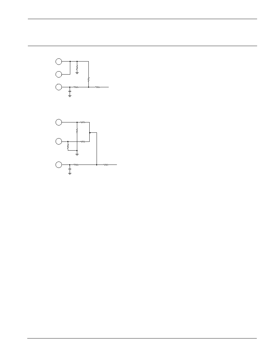
CURRENT LIMIT
There are two load current sensing pins, I SENSE A and I
SENSE B. The two pins can be shorted in the voltage mode
connection but both must be used in the current mode connec-
tion (see figures A and B). It is recommended that R
LIMIT
resistors be non-inductive. Load current flows in the I SENSE
pins. To avoid errors due to lead lengths connect the I LIMIT/
SHDN pin directly to the R
LIMIT
resistors (through the filter
network and shutdown divider resistor) and connect the R
LIMIT
resistors directly to the GND pin. Do not connect R
LIMIT
sense
resistors to the ground plane.
SA07
0
1
2
3
4
5
OUTPUT, I (A)
0
1
2
3
4
5
6
TOTAL VOLTAGE DROP
TOTAL VOLTAGE DROP, (V)
25
∞
C
≠55
∞
C ≠25
∞
C
125
∞
C
100
∞
C
85
∞
C
APEX MICROTECHNOLOGY CORPORATION ∑ TELEPHONE (520) 690-8600 ∑ FAX (520) 888-3329 ∑ ORDERS (520) 690-8601 ∑ EMAIL prodlit@apexmicrotech.com
Switching noise spikes will invariably be found at the I
SENSE pins. The noise spikes could trip the current limit
threshold which is only 100 mV. R
FILTER
and C
FILTER
should be
adjusted so as to reduce the switching noise well below 100
mV to prevent false current limiting. The sum of the DC level
plus the noise peak will determine the current limiting value. As
in most switching circuits it may be difficult to determine the
true noise amplitude without careful attention to grounding of
the oscilloscope probe. Use the shortest possible ground lead
for the probe and connect exactly at the GND terminal of the
amplifier. Suggested starting values are C
FILTER
= .001uF,
R
FILTER
= 5k .
The required value of R
LIMIT
in voltage mode may be calcu-
lated by:
R
LIMIT
= .1 V / I
LIMIT
where R
LIMIT
is the required resistor value, and I
LIMIT
is the
maximum desired current. In current mode the required value
of each R
LIMIT
is 2 times this value since the sense voltage is
divided down by 2 (see Figure B). If R
SHDN
is used it will further
divide down the sense voltage. The shutdown divider network
will also have an effect on the filtering circuit.
I SENSE A
I SENSE B
I LIMIT/SHDN
R
FILTER
C
FILTER
R
LIMIT
R
SHDN
SHUTDOWN
SIGNAL
1K
FIGURE A. CURRENT LIMIT WITH
SHUTDOWN VOLTAGE MODE.
I SENSE A
I SENSE B
I LIMIT/SHDN
R
FILTER
C
FILTER
R
SHDN
SHUTDOWN
SIGNAL
1K
1K
FIGURE B. CURRENT LIMIT WITH
SHUTDOWN CURRENT MODE.
R
LIMIT
R
LIMIT
SHUTDOWN
The shutdown circuitry makes use of the internal current
limiting circuitry. The two functions may be externally com-
bined in voltage and current modes as shown below in Figures
A and B. The R
LIMIT
resistors will normally be very low values
and can be considered zero for this application. In Figure A,
R
SHDN
and 1K form a voltage divider for the shutdown signal.
After a suitable noise filter is designed for the current limit,
adjust the value of R
SHDN
to give a minimum 110 mV of
shutdown signal at the I LIMIT/SHDN pin when the shutdown
signal is high. Note that C
FILTER
will filter both the current limit
noise spikes and the shutdown signal. Shutdown and current
limit operate on each cycle of the internal switching rate. As
long as the shutdown signal is high the output will be disabled.
PROTECTION CIRCUITS
Circuits monitor the temperature and load on each of the
bridge output transistors. On each cycle should any fault
condition be detected all output transistors in the bridge are
shut off. Faults protected against are: shorts across the out-
puts, shorts to ground, and over temperature conditions.
Should any of these faults be detected, the output transistors
will be latched off.* In addition there is a built in dead time
during which all the output transistors are off. The dead time
removes the possibility of a momentary conduction path through
the upper and lower transistors of each half bridge during the
switching interval. Noise or flyback may be observed at the
outputs during this time due to the high impedance of the
outputs in the off state. This will vary with the nature of the load.
OPERATING
CONSIDERATIONS
SA07
*
To restart the SA07 remove the fault and recycle V
CC
or,
alternatively, toggle the
I
LIMIT
/SHDN (PIN16) with a shut down
pulse.
This data sheet has been carefully checked and is believed to be reliable, however, no responsibility is assumed for possible inaccuracies or omissions. All specifications are subject to change without notice.
SA07U REV. B DECEMBER 1998
© 1998 Apex Microtechnology Corp.