 | –≠–ª–µ–∫—Ç—Ä–æ–Ω–Ω—ã–π –∫–æ–º–ø–æ–Ω–µ–Ω—Ç: SA18U | –°–∫–∞—á–∞—Ç—å:  PDF PDF  ZIP ZIP |

APEX MICROTECHNOLOGY CORPORATION ∑ TELEPHONE (520) 690-8600 ∑ FAX (520) 888-3329 ∑ ORDERS (520) 690-8601 ∑ EMAIL prodlit@apexmicrotech.com
SA18
USA
BeO
TE949311
FEATURES
∑ HALF BRIDGE IGBT OUTPUT
∑ WIDE SUPPLY RANGE--16-500V
∑ 20A TO 100
∞
C CASE
∑ 3 PROTECTION CIRCUITS
∑ SYNCHRONIZED OR EXTERNAL OSCILLATOR
∑ FLEXIBLE FREQUENCY CONTROL
APPLICATIONS
∑ MOTORS
∑ REACTIVE LOADS
∑ LOW FREQUENCY SONAR
∑ LARGE PIEZO ELEMENTS
∑ OFF-LINE DRIVERS
∑ C-D WELD CONTROLLER
DESCRIPTION
The SA18 is a pulse width modulation amplifier that can
supply 10KW to the load. An internal oscillator requires no
external components. The clock input stage divides the oscil-
lator frequency by two, which provides the switching fre-
quency of 22.5 kHz. External oscillators may also be used to
lower the switching frequency or to synchronize multiple
amplifiers. A shutdown input turns off both drivers of the half
bridge output. A high side current limit protects the amplifier
from shorts to ground in addition to load shorts. The output
IGBTs are protected from thermal overloads by directly sens-
ing the temperature of the die. The 12-pin hermetic MO-127
power package occupies only 3 square inches of board space.
BLOCK DIAGRAM AND TYPICAL APPLICATION
VOLTAGE CONTROLLED VOLTAGE SOURCE
EXTERNAL CONNECTIONS
H T T P : / / W W W . A P E X M I C R O T E C H . C O M ( 8 0 0 ) 5 4 6 - A P E X ( 8 0 0 ) 5 4 6 - 2 7 3 9
M I C R O T E C H N O L O G Y
PULSE WIDTH MODULATION AMPLIFIER
SA18
+V
S
NC
OUT
SHDN
NC
PWR GND
RSENSE
SIG GND
CLK IN
CONTROL
SIGNAL
3/7V
CLK OUT
FLAG
+PWM
Vcc
5V
5V
SHUTDOWN
CONTROL
OUTPUT
DRIVERS
PWM
56K
5K
.01
µ
F
470pF
˜
2
OSC
CURRENT
LIMIT
9
8
3
10
4
2
1
5
12
11
6
7
10V
P-P
LOAD
TOP
VIEW
CLK IN
CLK OUT
+PWM
FLAG
SIG GND
SHDN
NC
NC
+VS
VCC
*
*
OUT
PWR GND
1
2
3
4
5
6
12
11
10
9
8
7
TOP
VIEW
Case tied to pin 5. Allow no current in case. Bypassing of supplies
is required. Package is Apex MO≠127 (STD). See Outline
Dimensions/Packages in Apex data book.
As +PWM goes more positive, OUT duty cycle decreases.
*See text.
APEX MICROTECHNOLOGY CORPORATION ∑ 5980 NORTH SHANNON ROAD ∑ TUCSON, ARIZONA 85741 ∑ USA ∑ APPLICATIONS HOTLINE: 1 (800) 546-2739
PARAMETER
TEST CONDITIONS
2
MIN
TYP
MAX
UNITS
CLOCK (CLK)
CLK OUT, high level
4
I
OUT
1mA
4.8
5.3
V
CLK OUT, low level
4
I
OUT
1mA
0
.4
V
CLK IN, low level
4
0
.9
V
CLK IN, high level
4
3.7
5.4
V
FREQUENCY
44.10
45.00
45.9
kHz
ANALOG INPUT (+PWM)
center voltage
5
V
P-P voltage
0/100% modulation
4
V
FLAG
FLAG, high level
10
V
FLAG, low level
0
V
OUTPUT
TOTAL DROP
I = 20A
2.7
V
EFFICIENCY, 20A output
V
S
= 380V
98
%
SWITCHING FREQUENCY
OSC in
˜
2
22.05
22.50
22.95
kHz
CURRENT, continuous
4
100
∞
C case
20
A
CURRENT, peak
4
28
A
POWER SUPPLY
VOLTAGE, V
S
15
240
500
V
VOLTAGE, V
CC
14
15
16
V
CURRENT, V
CC
I
OUT
= 0
80
mA
CURRENT, V
CC,
shutdown
50
mA
CURRENT, V
S
No Load
45
mA
I
LIM
/SHUTDOWN
TRIP POINT
90
110
mV
INPUT CURRENT
100
nA
THERMAL
3
RESISTANCE, junction to case
1
∞
C/W
RESISTANCE, junction to air
12
∞
C/W
ABSOLUTE MAXIMUM RATINGS
SPECIFICATIONS
SA18
ABSOLUTE MAXIMUM RATINGS
SUPPLY VOLTAGE, +V
S
500V
SUPPLY VOLTAGE, V
CC
16V
POWER DISSIPATION, internal
1
125W
TEMPERATURE, pin solder - 10s
300
∞
C
TEMPERATURE, junction
2
150
∞
C
TEMPERATURE, storage
≠65 to +150
∞
C
OPERATING TEMPERATURE RANGE, case
≠55 to +125
∞
C
INPUT VOLTAGE, +PWM
0 TO +11V
INPUT VOLTAGE, SHDN
0 TO +11V
The SA18 is constructed from static sensitive components. ESD handling procedures must be observed.
The internal substrate contains beryllia (BeO). Do not break the seal. If accidentally broken, do not crush,
machine, or subject to temperatures in excess of 850
∞
C to avoid generating toxic fumes.
CAUTION
NOTES: 1.
Each of the two output transistors can dissipate 125W, but only one is on at any time.
2.
Unless otherwise noted: T
C
= 25
∞
C, V
S
, V
CC
at typical specification.
3.
Long term operation at the maximum junction temperature will result in reduced product life. Derate internal power
dissipation to achieve high MTTF. For guidance, refer to the heatsink data sheet.
4.
Guaranteed but not tested.
SPECIFICATIONS
APEX MICROTECHNOLOGY CORPORATION ∑ 5980 NORTH SHANNON ROAD ∑ TUCSON, ARIZONA 85741 ∑ USA ∑ APPLICATIONS HOTLINE: 1 (800) 546-2739
APEX MICROTECHNOLOGY CORPORATION ∑ TELEPHONE (520) 690-8600 ∑ FAX (520) 888-3329 ∑ ORDERS (520) 690-8601 ∑ EMAIL prodlit@apexmicrotech.com
SA18
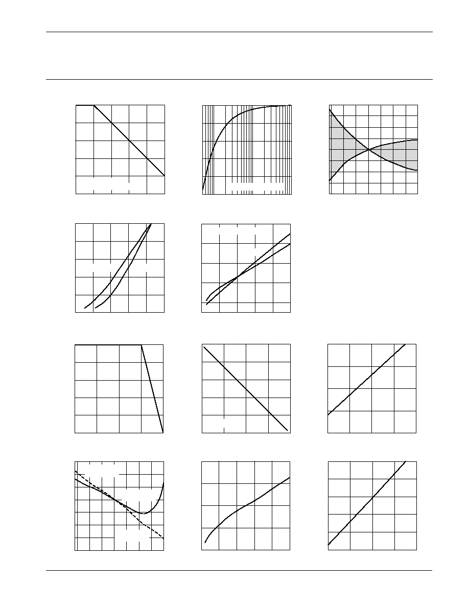
TYPICAL PERFORMANCE
GRAPHS
≠50 ≠25
0
25
50
75
100 125
80
85
90
95
100
105
110
115
1M
100K
95
98
99
100
CLOCK LOADING
96
97
10K
NORMALIZED FREQUENCY, (%)
CASE TEMPERATURE, (
∞
C)
CLOCK LOAD RESISTANCE, (
)
DUTY CYCLE VS ANALOG INPUT
DUTY CYCLE, (%)
0
20
40
60
80
100
ANALOG INPUT, (V)
3
5
4
7
6
Vcc QUIESCENT CURRENT
NORMALIZED Vcc QUIESCENT CURRENT, (%)
OUT
F NOMINAL = 45kHz
Vcc = 15V
F = 22.5 kHz
NORMAL
OPERATION
SHUTDOWN
OPERATION
≠50
CASE TEMPERATURE, (
∞
C)
CLOCK FREQUENCY OVER TEMP
NORMALIZED FREQUENCY, (%)
≠25
0
25
50
75 100 125
98.0
98.5
99.0
99.5
100
100.5
101.0
101.5
102.0
Vcc QUIESCENT CURRENT
NORMALIZED QUIESCENT CURRENT, (%)
0.5
DIODE FORWARD VOLTAGE DROP, (V)
REVERSE DIODE
FORWARD CURRENT, (A)
25
50
75
100
125
14
16
18
20
CONTINUOUS AMPS
12
1.0
1.5
2.0
3.0
2.5
5
0
100
200
300
400
500
25
10
15
20
CASE TEMPERATURE, (
∞
C)
CONTINUOUS AMPS, (A)
10
0
75
100
CASE TEMPERATURE, (
∞
C)
0
POWER DERATING
25
50
125
25
50
75
100
125
INTERNAL POWER DISSIPATION, (W)
SWITCHING FREQUENCY, F (kHz)
Vs, (V)
84
88
92
96
100
50
75
100
125
150
Vs QUIESCENT VS VOLTAGE
5
25
SWITCHING FREQUENCY, F (kHz)
60
70
50
80
90
Vs QUIESCENT VS FREQUENCY
NORMALIZED Vs QUIESCENT CURRENT, (%)
NORMALIZED Vs QUIESCENT CURRENT, (%)
100
10
15
20
EACH ACTIVE
OUTPUT TRANSISTOR
0
4
8
12
16
20
OUTPUT CURRENT, I(A)
1
1.5
2
2.5
3
TOTAL VOLTAGE DROP
TOTAL VOLTAGE DROP, (V)
100
∞
C
Tc = 100
∞
C
Tc = 25
∞
C
25
∞
C
CASE TEMPERATURE
20
0
4
8
12
16
This data sheet has been carefully checked and is believed to be reliable, however, no responsibility is assumed for possible inaccuracies or omissions. All specifications are subject to change without notice.
SA18U REV. B MARCH 2001
© 2001 Apex Microtechnology Corp.
rated output. The temperature of the output transistors is also
monitored. When either of the output transistors reaches
approximately 165
∞
C both are latched off. In either case, it will
be necessary to remove the fault condition and recycle power
to Vcc to restart the circuit. A short to +Vs can be protected
against by inserting a sensing resistor into the PWR GND
circuit as shown in Figure A.
In Figure A, the sense resistor inserted into the PWR GND
connection is tied to the SHDN pin. When the current from a
OPERATING
CONSIDERATIONS
SA18
GENERAL
Please read Application Note 30 on "PWM Basics". Refer to
Application Note 1 "General Operating Considerations" for
helpful information regarding power supplies, heat sinking and
mounting. Visit www.apexmicrotech.com for design tools that
help automate pwm filter design and heat sink selection. The
"Application Notes" and "Technical Seminar" sections contain
a wealth of information on specific types of applications.
Information on package outlines, heat sinks, mounting hard-
ware and other accessories are located in the "Packages and
Accessories" section. Evaluation Kits are available for most
Apex product models, consult the "Evaluation Kit" section for
details. For the most current version of all Apex product data
sheets, visit www.apexmicrotech.com.
CLOCK CIRCUIT AND RAMP GENERATOR
The clock frequency is internally set to a frequency of
approximately 45kHz. The CLK OUT pin will normally be tied
to the CLK IN pin. The clock is divided by two and applied to an
RC network which produces a ramp signal. An external clock
signal can be applied to the CLK IN pin for synchronization
purposes, but must be 45 kHz +/- 2%.
FLAG OUTPUT
Whenever the SA18 has detected a fault condition, the flag
output is set high (10V). When the programmable low side
current limit is exceeded, the FLAG output will be set high. The
FLAG output will be reset low on the next clock cycle. This
reflects the pulse-by-pulse current limiting feature. When the
internally-set high side current limit is tripped or the thermal
limit is reached, the FLAG output is latched high. See PRO-
TECTION CIRCUITS below.
PROTECTION CIRCUITS
A high side current monitor will latch off the output transistors
when the high side current rises to approximately 150% of
PWR GND
SHDN
R
SENSE
FIGURE A. PROTECTING AGAINST SHORTS TO +Vs.
R1
C1
short to +Vs develops 100 mV across the sense resistor the
shutdown circuit will shut off the output transistors for the
remainder of the switching cycle. The SA18 will restart at the
beginning of a new cycle and retest for this condition. This
circuit does not test for shorts to ground. The RC circuit R
1,
C
1
filters out any switching spikes and may need to be adjusted to
ignore normal current spikes in the application circuit.
An external shutdown command can be mixed with the
protection circuit of Figure A. In figure B a 10V shutdown
command signal is injected directly into the shutdown pin
(SHDN). As long as the shutdown command remains high both
output transistors will remain off.
BYPASSING
Adequate bypassing of the power supplies is required for
proper operation. Failure to do so can cause erratic and low
efficiency operation as well as excessive ringing at the outputs.
The Vs supply should be bypassed with at least a 1
µ
F ceramic
capacitor in parallel with another low ESR capacitor of at least
10
µ
F per amp of output current. Capacitor types rated for
switching applications are the only types that should be consid-
ered. The bypass capacitors must be physically connected
directly to the power supply pins. Even one inch of lead length
will cause excessive ringing at the outputs. This is due to the
very fast switching times and the inductance of the lead
connection. The bypassing requirements of the Vcc supply are
less stringent, but still necessary. A .1
µ
F to .47
µ
F ceramic
capacitor connected directly to the Vcc pin will suffice.
STARTUP CONDITIONS
The high side of the IGBT output bridge circuit is driven by
bootstrap circuit and charge pump arrangement. In order for
the circuit to produce a 100% duty cycle indefinitely the low
side of each half bridge circuit must have previously been in the
ON condition. This means, in turn, that if the input signal to the
SA18 at startup is demanding a 100% duty cycle, the output
may not follow the command and may be in a tri-state condi-
tion. The ramp signal must cross the input signal at some point
to correctly determine the output state. After the ramp crosses
the input signal level one time, the output state will be correct
thereafter.
PWR GND
SHDN
R
SENSE
SHUTDOWN
SIGNAL
FIGURE B. ADDING SHUTDOWN CONTROL.
C1
R1
R2
10V
IN4148