
1
32 to 40 SEC INSTANT VOICE ROM
FEATURES
* Voice length at
- 8 KHz sampling is 32 seconds
- 6 KHz sampling is 40 seconds
* Silence compression to save memory
* Eight trigger pins,TG1 to TG8 for 32 sections
* SBT pin play-all or sequential play-all
* 15 ms debounce time suitable for CDS
* IRP interrupt pin stops playback at once
* STP stop pulse generated at end of playback
* BUSY signal for CPU control
* Two LEDs flash at 3 Hz internal
* 3.0V to 6V single power supply operation
* Low standby current (<5
m
A at 3V)
* Auto-power down
* Built-in oscillator, D/A converter, EPROM
* ADPCM data compression
* Optional pop noise elimination function
* C
OUT
pin drives speaker with a transistor
* Development tools support
* V
OUT
1 and V
OUT
2 drives buzzer directly
* Sampling rate determined by external resistor
* Holdable and unholdable triggering option
* Industrial temperature available
GENERAL DESCRIPTION
API840N is a high-quality voice synthesizer with a capacity
of 32 to 40 seconds. A proprietary ADPCM algorithm is
used. The audio message is stored in a 1024-Kbit on-chip
EPROM.
The API840N eliminates the need of complicated circuitry
in voice playback (Figure 1) but still achieves high voice
quality. Sounds such as human speech, animal sounds,
musical sounds, and even special sound effects can be
synthesized. Devices can be cascaded to achieve longer
voice duration (Figure 3). Two devices can be configured
in parallel (Figure 4) in order to achieve signal mixing
without an external mixer allowing speeches to be mixed
with background music synthesis from two different chips.
The instant programming nature of the API840N allows a
very short production turnaround time. There are no NRE
charges that are usually required with conventional voice
ROMs. Users now can apply a voice synthesis function as
an additional feature to their products even when production
volume is relatively small. It is also ideal for trial or
engineering prototyping. As a result, the initial investment
is minimal and the risk in the product development phase
is reduced.
The API840N provides a wide voltage operating range
from 3.0V to 6.0V. A pair of PWM output pins, V
OUT
1 and
V
OUT
2 provide direct drive to a buzzer (Figure 2). Voice
quality from a buzzer is comparable to speaker output and
power consumption is much lower.
A current output pin, C
OUT
, enables the device to drive a
speaker with a low cost NPN transistor. No complex
filtering or amplifier circuit is needed. An automatic ramp
up/down function eliminates the undesired noise at the
end of playback.
Up to 32 sections are accessible through
TG1 to TG8
.The
SBT trigger pin can be programmed to playback all 32
sections or sequentially from section 1 to 32. An interrupt
pin (IRP) and stop pulse (STP) or BUSY signals provide
handshaking with microprocessors or other API840N
devices. All trigger pins give 15 ms debounce time and is
ideal for CDS applications as in Figure 6. Two LED drivers
are available, flashing on and off at approximately 3Hz
intervals (Figure 5). The internal voltage compensation
oscillator requires only one external resistor. Different
sampling frequencies are determined by the external
oscillator resistor value.
JUNE 1999
APLUS API840N

2
Programmable Options
The API840N provides different control functions for user
specified applications. They include:
* Non-sequential or Sequential Play-all
* Unholdable or Holdable trigger
* STOP or BUSY signal selection
* Automatic ramp-up/ramp-down or no ramp-up/ramp-down
OSCILLATOR
OSC
CLOCK
GENERATOR
CONTROL
LOGIC
TG1
TG8
SBT
IRP
LED
DRIVER
LED2
LED1
STP
POP NOISE
REDUCTION
ADDRESS
SEQUENCER
VOICE
EPROM
ADPCM
DECODER
BUZZER
BUFFER
D/A
C
OUT
V
OUT1
V
OUT2
GND
Vcc
BLOCK DIAGRAM
OPERATING RANGE
Range
Ambient Temp.
Vcc
Commercial
0
�
C to +70
�
C 3.0V to 5.0V
Industrial
-40
�
C to +85
�
C 3.0V to 5.0V
ABSOLUTE MAXIMUM RATINGS
(1)
Symbol
Parameter
Value
Unit
V
TERM
Terminal Voltage with Respect to GND
-0.5 to +7.0
V
T
BIAS
Temperature Under Bias
-40 to +85
�
C
T
STG
Storage Temperature
-55 to +125
�
C
Notes:
1. Stress greater than those listed under ABSOLUTE MAXIMUM RATINGS may cause permanent damage to the
device. This is a stress rating only and functional operation of the device at these or any other conditions above
those indicated in the operational sections of this specification is not implied. Exposure to absolute maximum
rating conditions for extended periods may affect reliability.
Silence Compression
If a particular sound sequence includes periods of silence,
the API840N will automatically compress the silence to
save memory space. This compression will not affect
playback of the sound sequence.
APLUS API840N

3
SECTION TRIGGERING
TG1
TG2
TG3
TG4
TG5
TG6
TG7
TG8
Section
HIGH
NC
NC
NC
NC
NC
NC
NC
1
NC
HIGH
NC
NC
NC
NC
NC
NC
2
NC
NC
HIGH
NC
NC
NC
NC
NC
3
NC
NC
NC
HIGH
NC
NC
NC
NC
4
NC
NC
NC
NC
HIGH
NC
NC
NC
5
NC
NC
NC
NC
NC
HIGH
NC
NC
6
NC
NC
NC
NC
NC
NC
HIGH
NC
7
NC
NC
NC
NC
NC
NC
NC
HIGH
8
HIGH
HIGH
NC
NC
NC
NC
NC
NC
9
NC
HIGH
HIGH
NC
NC
NC
NC
NC
10
NC
NC
HIGH
HIGH
NC
NC
NC
NC
11
NC
NC
NC
HIGH
HIGH
NC
NC
NC
12
NC
NC
NC
NC
HIGH
HIGH
NC
NC
13
NC
NC
NC
NC
NC
HIGH
HIGH
NC
14
NC
NC
NC
NC
NC
NC
HIGH
HIGH
15
HIGH
NC
NC
NC
NC
NC
NC
HIGH
16
HIGH
HIGH
HIGH
NC
NC
NC
NC
NC
17
NC
HIGH
HIGH
HIGH
NC
NC
NC
NC
18
NC
NC
HIGH
HIGH
HIGH
NC
NC
NC
19
NC
NC
NC
HIGH
HIGH
HIGH
NC
NC
20
NC
NC
NC
NC
HIGH
HIGH
HIGH
NC
21
NC
NC
NC
NC
NC
HIGH
HIGH
HIGH
22
HIGH
NC
NC
NC
NC
NC
HIGH
HIGH
23
HIGH
HIGH
NC
NC
NC
NC
NC
HIGH
24
HIGH
HIGH
HIGH
HIGH
NC
NC
NC
NC
25
NC
HIGH
HIGH
HIGH
HIGH
NC
NC
NC
26
NC
NC
HIGH
HIGH
HIGH
HIGH
NC
NC
27
NC
NC
NC
HIGH
HIGH
HIGH
HIGH
NC
28
NC
NC
NC
NC
HIGH
HIGH
HIGH
HIGH
29
HIGH
NC
NC
NC
NC
HIGH
HIGH
HIGH
30
HIGH
HIGH
NC
NC
NC
NC
HIGH
HIGH
31
HIGH
HIGH
HIGH
NC
NC
NC
NC
HIGH
32
APLUS API840N
4
PIN DESCRIPTIONS
Name
I/O
Function
TG8
I
Trigger Switch 8, Internal Pull LOW,
Active HIGH
O
Drives First LED Flash at 3 Hz,
Active LOW
V
OUT1
O
PWM Audio Signal Output for
Buzzer
V
OUT2
O
Compliment PWM Audio Signal
Output for Buzzer
GND
-
Power Ground
STP/BUSY
O
Generate 30 ms Pulse or Busy
Signal After Voice Playback
O
Drives Second LED Flash at 3 Hz,
Active LOW
C
OUT
O
Current Output from Internal DAC
for Speaker Playback
OSC
I
Oscillator Resistor Pin to Control
Sampling Frequency
TG5
I
Trigger Switch 5, Internal Pull LOW,
Active HIGH
TG6
I
Trigger Switch 6, Internal Pull LOW,
Active HIGH
V
PP
-
Program Power Supply, No
Connect When Voice Playback
TG1
I
Trigger Switch 1, Internal Pull LOW,
Active HIGH
TG2
I
Trigger Switch 2, Internal Pull LOW,
Active HIGH
V
CC
-
Positive Power Supply
TG3
I
Trigger Switch 3, Internal Pull LOW,
Active HIGH
TG4
I
Trigger Switch 4, Internal Pull LOW,
Active HIGH
SBT
I
One Key or Sequential Trigger,
Internal Pull LOW, Active HIGH
IRP
I
Interrupt to Stop Playback, Internal
Pull LOW, Active HIGH
TG7
I
Trigger Switch 7, Internal Pull LOW,
Active HIGH
Note:
1. The following pins are used to program data into the memory on the chip:
pins 5, 6, 7, 9, 12, 15, 18 and 19.
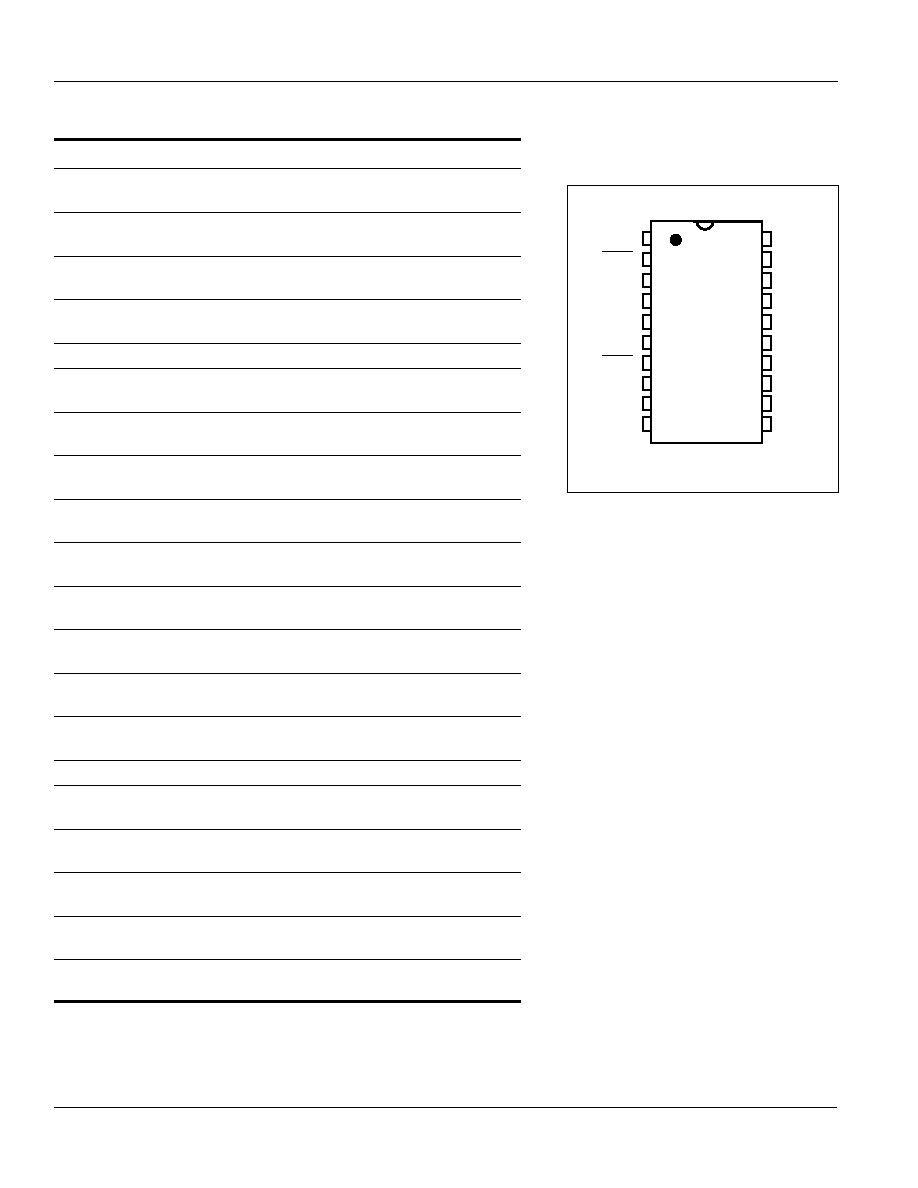
PIN CONFIGURATION
20-Pin 300-mil PDIP
1
2
3
4
5
6
7
8
9
10
20
19
18
17
16
15
14
13
12
11
TG8
LED1
V
OUT1
V
OUT2
GND
STP
LED2
C
OUT
OSC
TG5
TG7
IRP
SBT
TG4
TG3
V
CC
TG2
TG1
V
PP
TG6
APLUS API840N
LED 1
LED 2
5
DC CHARACTERISTICS
Symbol
Parameter Description
Condition
Min.
Typ.
Max.
Unit
V
CC
Operating Voltage 3.0 4.5 5.0 V
I
SB
Standby Current
V
CC
= 3.0V, I/O Open
-
1
5
m
A
I
OP
Operating Current
Vcc
= 3.0V, I/O Open
-
-
100
m
A
V
IH
Input HIGH Voltage
Vcc
= 3.0V
2.5
3.0
3.5
V
V
IL
Input LOW Voltage
Vcc
= 3.0V
-0.3
0
0.3
V
I
OH
V
OUT
LOW O/P Current
Vcc
= 3.0V, V
OUT
= 0V
-
-12
-
mA
I
OL
V
OUT
HIGH O/P Current
Vcc = 3.0V, V
OUT
= 3.0V
-
12
-
mA
I
CO
C
OUT
O/P Current
Vcc
= 3.0V, V
COUT
= 0.7V
-
- 2
-
mA
I
STPH
STP LOW O/P Current
Vcc
= 3.0V, V
STP
= 0V
-
- 5
-
mA
T
STPL
STP HIGH O/P Current
Vcc
= 3.0V, V
STP
= 3.0V
-
5
-
mA
I
LED
Output Current LED
Vcc = 3.0V - 6.0V
6
8
10
mA
D
F/F
Frequency Stability
F
OSC
(3V) - F
OSC
(3.5V)
-
-
5
%
F
OSC
(3V)
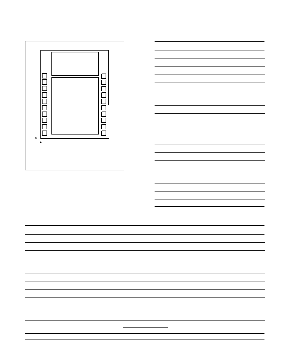
BONDING PARAMETERS
Pin
Name
X
Y
1
TG8
3451.9
1599.7
2
3451.9
1861.0
3
V
OUT1
3451.9
2147.6
4
V
OUT2
3451.9
2444.5
5
GND
3368.10
2803.35
6
STP
137.18
2795.93
7
100.4
2486.3
8
C
OUT
100.4
2245.0
9
OSC
100.4
1790.0
10
TG5
100.4
1469.5
11
TG6
100.4
1230.0
12
V
PP
100.4
989.6
13
TG1
100.4
662.3
14
TG2
100.4
422.7
15
V
CC
187.05
113.78
16
TG3
3372.5
141.8
17
TG4
3451.9
581.5
18
SBT
3451.9
836.0
19
IRP
3451.9
1090.6
20
TG7
3451.94
1345.13
BONDING DIAGRAM
(0,0)
X
Y
Note: Substrate must be connected to GND
Pad size = 100
m
m x 100
m
m
5
4
3
2
1
20
19
18
17
16
6
7
8
9
10
11
12
13
14
15
APLUS API840N
LED1
LED2
Die size:3628
m
m x 3797
m
m