 | –≠–ª–µ–∫—Ç—Ä–æ–Ω–Ω—ã–π –∫–æ–º–ø–æ–Ω–µ–Ω—Ç: AX88790 | –°–∫–∞—á–∞—Ç—å:  PDF PDF  ZIP ZIP |
ASIX ELECTRONICS CORPORATION Frist Released Date : Jun/19/2000
2F, NO.13, Industry East Rd. II, Science-based Industrial Park, Hsin-Chu City, Taiwan, R.O.C.
TEL: 886-3-579-9500
FAX: 886-3-579-9558 http://www.asix.com.tw
AX88790 L
3-in-1 PCMCIA Fast Ethernet Controller
10/100BASE 3-in-1 PCMCIA Fast Ethernet Controller
Document No.: AX790-15 / V1.5 / Jan. 24 '02
Features
∑
Highly integrated with embedded 10/100Mbps
MAC, PHY and Transceiver
∑
Compliant with IEEE 802.3/802.3u
100BASE-TX/FX specification
∑
Single chip PCMCIA bus 10/100Mbps Fast
Ethernet MAC Controller
∑
Embedded 8K * 16 bit SRAM
∑
NE2000 register level compatible instruction
∑
Compliant with 16 bit PC Card Standard -
February 1995
∑
Support both 10Mbps and 100Mbps data rate
∑
Support both full-duplex or half-duplex operation
∑
Provides FAX/MODEM interface for COMBO AP
∑
Provides an extra MII port for supporting other
media. For example, Home-LAN application
∑
Support 128/256 bytes EEPROM (used for saving
CIS)
∑
Support automatic loading of Ethernet ID, CIS and
Adapter Configuration from EEPROM on
power-on initialization
∑
External and internal loop-back capability
∑
Support 3 General Purpose Input pins
∑
Low Power Consumption, typical under 100mA
∑
128-pin LQFP low profile package
∑
0.25 Micron low power CMOS process. 25MHz
Operation, Pure 3.3V operation with 5V I/O
tolerance.
*IEEE is a registered trademark of the Institute of Electrical and Electronic
Engineers, Inc.
*All other trademarks and registered trademark are the property of their
respective holders.
Product description
The AX88790 Fast Ethernet Controller is a high performance and highly integrated PCMCIA bus Ethernet Controller
with embedded 10/100Mbps PHY/Transceiver and 8K*16 bit SRAM. The AX88790 contains a 16 bit PCMCIA
interfaces to host CPU and compliant with PC Card Standard ≠ February 1995. The AX88790 implements both 10Mbps
and 100Mbps Ethernet function based on IEEE802.3 / IEEE802.3u LAN standard. The AX88790 also provides an extra
IEEE802.3u compliant media-independent interface (MII) to support other media applications. Using MII interface,
Home LAN PHY type media can be supported. The AX88790 is built in interface to connect FAX/MODEM chipset with
parallel bus interface.
Typical System Block Diagram
Always contact ASIX for possible updates before starting a design.
This data sheet contains new products information. ASIX ELECTRONICS reserves the rights to modify product specification without notice. No liability
is assumed as a result of the use of this product. No rights under any patent accompany the sale of the product.
AX88790 with 10/100 PHY/TxRx
MODEM
DAA
MAGNETIC
RJ45
RJ11
PCMCIA I/F
EEPROM
Home LAN PHY
/TxRx
MAGNETIC
RJ11

ASIX ELECTRONICS CORPORATION
2
AX88790 L 3-in-1 PCMCIA Fast Ethernet Controller
CONTENTS
1.0 INTRODUCTION .............................................................................................................................................. 5
1.1 G
ENERAL
D
ESCRIPTION
:..................................................................................................................................... 5
1.2 AX88790 B
LOCK
D
IAGRAM
: .............................................................................................................................. 5
1.3 AX88790 P
IN
C
ONNECTION
D
IAGRAM
............................................................................................................... 6
2.0 SIGNAL DESCRIPTION ................................................................................................................................... 7
2.1 PCMCIA B
US
I
NTERFACE
S
IGNALS
G
ROUP
......................................................................................................... 7
2.2 EEPROM S
IGNALS
G
ROUP
................................................................................................................................ 8
2.3 MII
INTERFACE SIGNALS GROUP
.......................................................................................................................... 8
2.4 10/100M
BPS
T
WISTED
-P
AIR
I
NTERFACE PINS GROUP
........................................................................................... 9
2.5 B
UILT
-
IN
PHY LED
INDICATOR PINS GROUP
....................................................................................................... 9
2.6 M
ODEM INTERFACE PINS GROUP
.......................................................................................................................... 9
2.7 G
ENERAL
P
URPOSE
I/O
PINS GROUP
.................................................................................................................. 10
2.8 M
ISCELLANEOUS PINS GROUP
............................................................................................................................ 11
2.9 P
OWER ON CONFIGURATION SETUP SIGNALS CROSS REFERENCE TABLE
................................................................ 12
3.0 MEMORY AND I/O MAPPING...................................................................................................................... 13
3.1 EEPROM M
EMORY
M
APPING
.......................................................................................................................... 13
3.2 A
TTRIBUTE
M
EMORY
M
APPING
........................................................................................................................ 13
3.3 I/O M
APPING
................................................................................................................................................... 14
3.4 SRAM M
EMORY
M
APPING
.............................................................................................................................. 14
4.0 REGISTERS OPERATION ............................................................................................................................. 15
4.1 PCMCIA F
UNCTION
C
ONFIGURATION
R
EGISTER
S
ET OF
LAN........................................................................... 15
4.1.1 Configuration Option Register of LAN (LCOR) Offset 3C0H (Read/Write) ............................................... 16
4.1.2 Configuration and Status Register of LAN (LCSR) Offset 3C2H (Read/Write) ......................................... 17
4.1.3 I/O Base Register 0/1 of LAN (LIOBASE0/1) Offset 3CAH/3CCH (Read/Write) ...................................... 17
4.2 PCMCIA F
UNCTION
C
ONFIGURATION
R
EGISTER
S
ET OF
MODEM .................................................................... 18
4.2.1 Configuration Option Register of MODEM (MCOR) Offset 3E0H (Read/Write) ...................................... 18
4.2.2 Configuration and Status Register of MODEM (MCSR) Offset 3E2H (Read/Write) ................................. 19
4.2.3 I/O Base Register 0/1 of MODEM (MIOBASE0/1) Offset 3EAH/3ECH (Read/Write) .............................. 19
4.3 MAC C
ORE
R
EGISTERS
.................................................................................................................................... 20
4.3.1 Command Register (CR) Offset 00H (Read/Write) ................................................................................... 22
4.3.2 Interrupt Status Register (ISR) Offset 07H (Read/Write) .......................................................................... 22
4.3.3 Interrupt mask register (IMR) Offset 0FH (Write).................................................................................... 23
4.3.4 Data Configuration Register (DCR) Offset 0EH (Write) .......................................................................... 23
4.3.5 Transmit Configuration Register (TCR) Offset 0DH (Write) .................................................................... 23
4.3.6 Transmit Status Register (TSR) Offset 04H (Read)................................................................................... 24
4.3.7 Receive Configuration (RCR) Offset 0CH (Write).................................................................................... 24
4.3.8 Receive Status Register (RSR) Offset 0CH (Read) ................................................................................... 24
4.3.9 Inter-frame gap (IFG) Offset 16H (Read/Write)....................................................................................... 24
4.3.10 Inter-frame gap Segment 1(IFGS1) Offset 12H (Read/Write) ................................................................. 25
4.3.11 Inter-frame gap Segment 2(IFGS2) Offset 13H (Read/Write) ................................................................. 25
4.3.12 MII/EEPROM Management Register (MEMR) Offset 14H (Read/Write)................................................. 25
4.3.13 Test Register (TR) Offset 15H (Write) .................................................................................................... 25
4.3.14 Test Register (TR) Offset 15H (Read) .................................................................................................... 25
4.3.15 General Purpose Input Register (GPI) Offset 17H (Read)...................................................................... 26
4.3.16 GPO and Control (GPOC) Offset 17H (Write) ....................................................................................... 26
4.4 T
HE
E
MBEDDED
PHY R
EGISTERS
..................................................................................................................... 27
4.4.1 MR0 -- Control Register Bit Descriptions................................................................................................. 28
4.4.2 MR1 -- Status Register Bit Descriptions ................................................................................................... 29
4.4.3 MR2, MR3 -- Identification Registers (1 and 2) Bit Descriptions.............................................................. 30
4.4.4 MR4 ≠ Autonegotiation Advertisement Registers Bit Descriptions............................................................ 30
4.4.5 MR5 ≠ Autonegotiation Link Partner Ability (Base Page) Register Bit Descriptions................................. 30

ASIX ELECTRONICS CORPORATION
3
AX88790 L 3-in-1 PCMCIA Fast Ethernet Controller
4.4.6 MR5 ≠Autonegotiation Link Partner (LP) Ability Register (Next Page) Bit Descriptions .......................... 31
4.4.7 MR6 ≠ Autonegotiation Expansion Register Bit Descriptions ................................................................... 31
4.4.8 MR7 ≠Next Page Transmit Register Bit Descriptions ............................................................................... 32
4.4.9 MR16 ≠ PCS Control Register Bit Descriptions........................................................................................ 32
4.4.10 MR17 ≠Autonegotiation Register A Bit Descriptions .............................................................................. 33
4.4.11 MR18 ≠Autonegotiation Register B Bit Descriptions .............................................................................. 33
4.4.12 MR20 ≠User Defined Register Bit Descriptions...................................................................................... 33
4.4.13 MR21 ≠RXER Counter Register Bit Descriptions ................................................................................... 34
4.4.14 MR28 ≠Device-Specific Register 1 (Status Register) Bit Descriptions..................................................... 34
4.4.15 MR29 ≠Device-Specific Register 2 (100Mbps Control) Bit Descriptions................................................. 35
4.4.16 MR30 ≠Device-Specific Register 3 (10Mbps Control) Bit Descriptions................................................... 36
4.4.17 MR31 ≠Device-Specific Register 4 (Quick Status) Bit Descriptions ........................................................ 37
5.0 DEVICE ACCESS FUNCTIONS .................................................................................................................... 38
5.1 PCMCIA
INTERFACE ACCESS FUNCTIONS
.......................................................................................................... 38
5.1.1 Attribute Memory access function functions. ............................................................................................ 38
5.1.1 I/O access function functions.................................................................................................................... 38
5.2 MII S
TATION
M
ANAGEMENT FUNCTIONS
. ......................................................................................................... 39
6.0 ELECTRICAL SPECIFICATION AND TIMINGS....................................................................................... 40
6.1 A
BSOLUTE
M
AXIMUM
R
ATINGS
........................................................................................................................ 40
6.2 G
ENERAL
O
PERATION
C
ONDITIONS
................................................................................................................... 40
6.3 DC C
HARACTERISTICS
..................................................................................................................................... 40
6.4 A.C. T
IMING
C
HARACTERISTICS
....................................................................................................................... 41
6.4.1 XTAL / CLOCK ........................................................................................................................................ 41
6.4.2 Reset Timing ............................................................................................................................................ 41
6.4.3 Attribute Memory Read Timing ................................................................................................................ 43
6.4.4 Attribute Memory Write Timing................................................................................................................ 44
6.4.5 I/O Read Timing....................................................................................................................................... 45
6.4.6 I/O Write Timing ...................................................................................................................................... 46
6.4.7 MII Timing............................................................................................................................................... 47
7.0 PACKAGE INFORMATION........................................................................................................................... 48
APPENDIX A: APPLICATION NOTE 1 ............................................................................................................. 49
A.1 U
SING
C
RYSTAL
25MH
Z
................................................................................................................................. 49
A.2 U
SING
O
SCILLATOR
25MH
Z
............................................................................................................................ 49
APPENDIX B: POWER CONSUMPTION REFERENCE DATA...................................................................... 50
ERRATA OF AX88790 .......................................................................................................................................... 51
DEMONSTRATION CIRCUIT (A) : AX88790 + HOMEPNA 1M8 PHY.......................................................... 52
DEMONSTRATION CIRCUIT (B) : AX88790 ONLY ....................................................................................... 57

ASIX ELECTRONICS CORPORATION
4
AX88790 L 3-in-1 PCMCIA Fast Ethernet Controller
FIGURES
F
IG
- 1 AX88790 B
LOCK
D
IAGRAM
............................................................................................................................. 5
F
IG
- 2 AX88790 P
IN
C
ONNECTION
D
IAGRAM
.............................................................................................................. 6
TABLES
T
AB
- 1 PCMCIA
BUS INTERFACE SIGNALS GROUP
........................................................................................................ 7
T
AB
- 2 EEPROM
BUS INTERFACE SIGNALS GROUP
....................................................................................................... 8
T
AB
- 3 MII
INTERFACE SIGNALS GROUP
....................................................................................................................... 8
T
AB
- 4 10/100M
BPS
T
WISTED
-P
AIR
I
NTERFACE PINS GROUP
......................................................................................... 9
T
AB
- 5 B
UILT
-
IN
PHY LED
INDICATOR PINS GROUP
.................................................................................................... 9
T
AB
- 6 M
ODEM INTERFACE SIGNALS GROUP
............................................................................................................... 10
T
AB
≠ 7 G
ENERAL
P
URPOSES
I/O
PINS GROUP
............................................................................................................. 10
T
AB
≠ 8 M
ISCELLANEOUS PINS GROUP
........................................................................................................................ 11
T
AB
- 9 P
OWER ON
C
ONFIGURATION
S
ETUP
T
ABLE
..................................................................................................... 12
T
AB
≠ 10 EEPROM M
EMORY
M
APPING
.................................................................................................................... 13
T
AB
≠ 11 A
TTRIBUTE
M
EMORY
M
APPING
................................................................................................................... 13
T
AB
≠ 12 I/O A
DDRESS
M
APPING
............................................................................................................................... 14
T
AB
≠ 13 L
OCAL
M
EMORY
M
APPING
.......................................................................................................................... 14
T
AB
≠ 14 PCMCIA F
UNCTION
C
ONFIGURATION
R
EGISTER
M
APPING OF
LAN ............................................................. 15
T
AB
≠ 15 PCMCIA F
UNCTION
C
ONFIGURATION
R
EGISTER
M
APPING OF
MODEM ...................................................... 18
T
AB
- 16 P
AGE
0
OF
MAC C
ORE
R
EGISTERS
M
APPING
................................................................................................ 20
T
AB
- 17 P
AGE
1
OF
MAC C
ORE
R
EGISTERS
M
APPING
................................................................................................ 21
T
AB
≠ 18 T
HE
E
MBEDDED
PHY R
EGISTERS
................................................................................................................ 27
T
AB
- 19 MII M
ANAGEMENT
F
RAME
F
ORMAT
............................................................................................................ 39
T
AB
- 20 MII M
ANAGEMENT
F
RAMES
-
FIELD
D
ESCRIPTION
......................................................................................... 39

ASIX ELECTRONICS CORPORATION
5
AX88790 L 3-in-1 PCMCIA Fast Ethernet Controller
1.0 Introduction
1.1 General Description:
The AX88790 provides industrial standard NE2000 registers level compatible instruction set. Various drivers are easy
acquired, maintenance and usage with no pain and tears
The AX88790 Fast Ethernet Controller is a high performance and highly integrated PCMCIA bus Ethernet Controller
with embedded 10/100Mbps PHY/Transceiver and 8K*16 bit SRAM. The AX88790 contains a 16 bit PCMCIA
interfaces to host CPU and compliant with PC Card Standard ≠ February 1995. The AX88790 implements both 10Mbps
and 100Mbps Ethernet function based on IEEE802.3 / IEEE802.3u LAN standard. The AX88790 also provides an extra
IEEE802.3u compliant media-independent interface (MII) to support other media applications. Using MII interface,
Home LAN PHY type media can be supported. The AX88790 is also built in interface to connect FAX/MODEM chipset
with parallel bus interface.
The main difference between AX88790 and AX88190 are: 1) Embedded packet buffer memory 2) Built-in 10/100Mbps
PHY/Transceiver 3) Replace memory I/F with PHY/Transceiver I/F. 4) Fix OE# signal synchronous problem 5) Fix
interrupt status can't always clean up problem of AX88190. 6) Add 3 general-purpose input pins.
AX88790 use 128-pin LQFP low profile package, 25MHz operation, and single 3.3V operation with 5V I/O tolerance.
The ultra low power consumption is an outstanding feature and enlarges the application field. It is suitable for some
power consumption sensitive product like Compact Flash Adapter Card, PDA (Personal Digital Assistant) and Palm size
computer ...etc.
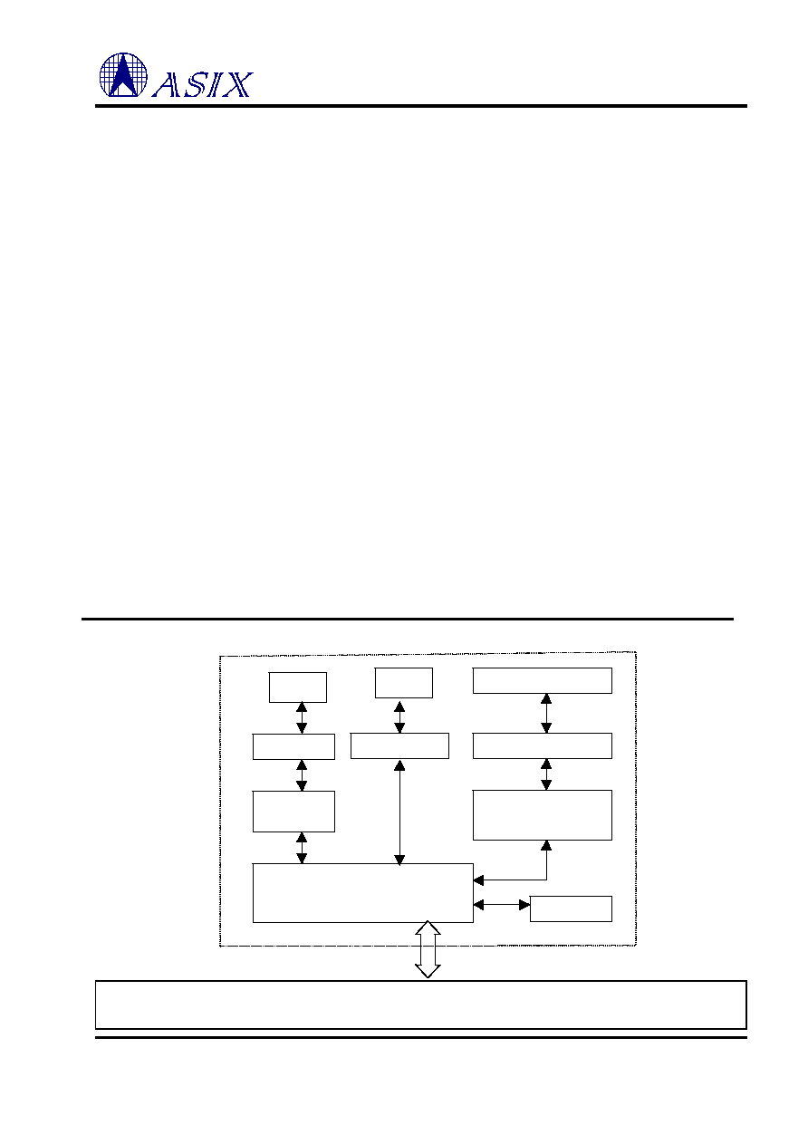
1.2 AX88790 Block Diagram:
Fig - 1 AX88790 Block Diagram
MAC
Core
&
PHY
8K* 16 SRAM
and Memory Arbiter
Remote
DMA
FIFOs
NE2000/GPI
Registers
PCMCIA Interface
STA
SEEPROM
LOADER I/F
SD[15:0]
SA[9:0]
Ctl BUS
MII I/F
SMDC
SMDIO
EECS
EECK
EEDI
EEDO
MODEM
I/F
TPI, TPO
GPI