257
www.ptcc.com.tw
SEMICONDUCTOR
Pin Configuration ≠
Top View
AS1717D
MON
GND
CLAD
REGA
G2
G1
OVAD
OPAD
COMP
CL
FB
VC
OV
MAR1
MAR2
CSET
AS1717D
V Adjust and Current Limit
Preliminary Specification
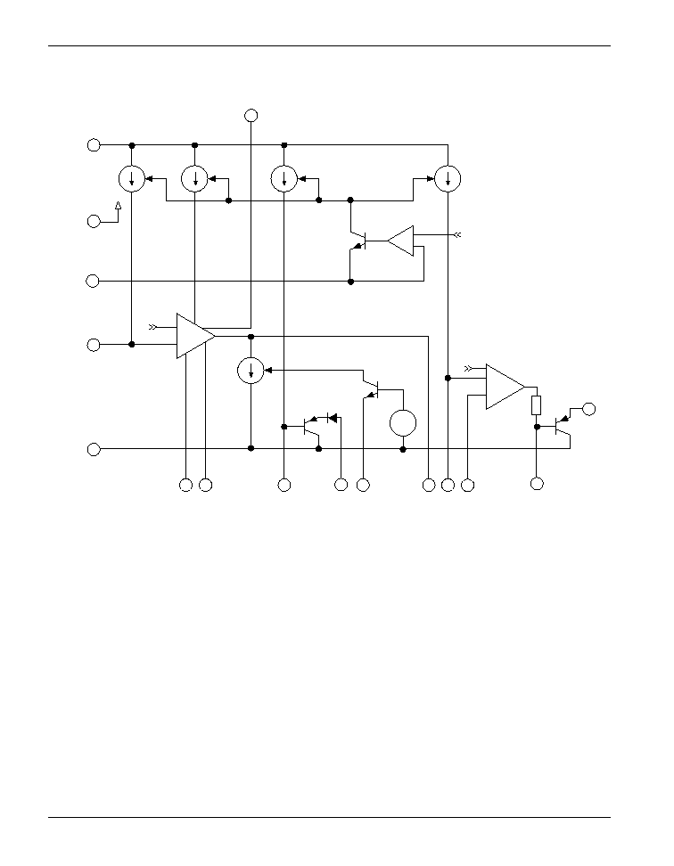
The AS1717D is a 16 pin surface mount IC implementing the Astec Linear Programming architecture (ALPTM)
incorporating the current limit, voltage adjustment and overvoltage programming functions for an AMPSSTM module.
These features can be programmed with external resistors or with voltage inputs. To accomplish this, the control
inputs CLAD, OPAD, and OVAD (for current limit, output adjust, and overvoltage adjust respective) include on chip
current sources.
The output voltage adjust circuit is a transconductance amplifier. Within its normal operating range, it measures the
difference between the OPAD pin and 2.0V, and can source/sink a current proportional to this voltage into the
systems main feedback node. A second identical current is generated which is fed into the system's overvoltage node
to cause the OV detection circuitry to track the output voltage. An additional current is generated by the OVAD
circuitry to add an additional offset current to the OV output.
The current limit amplifier is a differential amplifier which responds to the difference between the systems current
monitor CMON and the programmed current limit CLAD. The module current limit is intended to be implemented as a
closed loop, giving constant output current equal to the programmed value. The current limit amp has a fixed gain,
and a common mode correction circuit sets the nominal output voltage based on the programmed current limit value.
The output of this amplifier is current sinking only and is intended to wire-OR with the error amplifier in an AS2842
series PWM controller.
Description
Ordering Information
259
www.ptcc.com.tw
AS1717D
V Adjust and Current Limit
Pin Function Description
Pin Number
Function
Description
1
COMP
Low impedance output of current limit amp.
2
CL
Filterable output of current limit amp.
3
FB
Output of V adjust circuit, output current is proportional to
(OPAD - 2V) up to ±500µA, with a gain set by a resistor from
G1 to G2.
4
VC
Positive supply input.
5
OV
Output of V adjust and OV adjust circuits, output current is pro-
portional to (OPAD - 2V) plus the current programmed by
OVAD pin.
6
MAR1
A resistor from MAR1 to MAR2 sets the OV adjust range.
7
MAR2
8
CSET
Input pin for setting on-chip current sources. Chip forces this
pin to 1.5V, a 1.43k
resistor to ground sets normal chip oper-
ation, biasing most current sources to 1mA.
9
OPAD
Output adjust input. A 1 mA current source pulls this pin posi
tive with resistive or open loading.
10
OVAD
1 mA current source for overvoltage linear adjust circuitry. The
voltage at this pin (0-1V) also programs a current to the OV
output.
11
G1
Resistor from G1 to G2 sets transconductance of voltage
adjust circuitry.
12
G2
13
REGA
5.0V voltage reference input.
14
CLAD
Current limit adjust input. A 1 mA current source pulls this pin
positive with resistive or open loading.
15
GND
Signal ground and silicon substrate.
16
MON
Input to current limit from current sensing circuit.
Absolute Maximum Ratings
Parameter
Symbol
Rating
Unit
Supply Voltage
VCC
20
V
Continuous Power
PD
1000
mW
Junction Temperature
TJ
150
∞C
Storage Temperature
TSTG
≠60 to +150
∞C
Lead Temperature (Soldering, 10 seconds)
TL
300
∞C
260
www.ptcc.com.tw
AS1717D
V Adjust and Current Limit
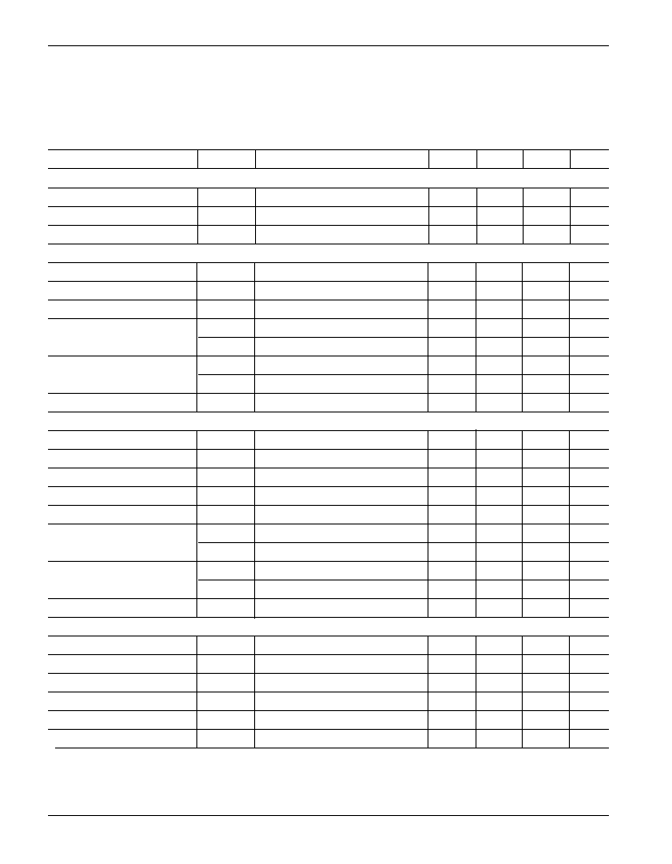
Electrical Characteristics
Electrical characteristics are guaranteed over the full junction temperature range (-20 -105∞C). Ambient temperature must be der-
ated based upon power dissipation and package thermal characteristics. The conditions are: 10
VC
16V; REGA = 5V; FB =
2V5; CLAD = 2V5; OPAD = 2V5; MON = 2V; OV = 2V5; ICOMP = 1mA; 750
MAR1 to MAR2; 1k43 CSET to GND, unless other-
wise specified.
Parameter
Symbol
Test Condition
Min.
Typ.
Max.
Unit
Bias (VCC, VREG, CSET)
Supply Current
IC
9
13
mA
Reference Current
IREGA
1
3
mA
CSET Reference
VCSET
1.47
1.5
1.53
V
Output Adjust
Program Current
IOPAD
-0.95
-1
-1.05
mA
Clamp Voltage
VOPAD
Open Circuit
5.3
5.6
6.1
V
Input Null Voltage
VOS
VG1-VG2 @ OPAD = 2.03 V
-30
30
mV
FB Output Null Current
IFBB
G1, G2 Open Circuit
-10
10
µA
IFPO
G1 = G2; OPAD Open
-2
2
µA
FB Output Current
IFBP
G1 = G2, OPAD = 2.5V
430
475
530
µA
IFBN
G1 = G2, OPAD = 1.5V
-430
-475
-530
µA
FB Transfer Gain
IFBD
IG1 = 200 µA; 1G2 = 200 µA
180
200
220
µA
Overvoltage Adjust
Program Current
IOVAD
-0.95
-1
-1.05
mA
Clamp Voltage
VOVAD
Open Circuit
5.3
5.6
6.1
V
OV Current
IOV
OVAD = 0V;
700
780
900
µA
OV Gain
GOV
0 < VOVAD <600mV
.775
.875
.975
mA/V
Gain Set Voltage
VOVAD
MAR2 - MAR1 (25∞C)
623
mV
OV Output Null Current
IOVB
G1, G2 Open Circuit
-10
10
µA
IOVO
G1 = G2; OPAD Open
-2
2
µA
OV Output Current
IOVP
G1 = G2, OPAD = 2.5V
430
475
530
µA
IOVN
G1 = G2; OPAD = 1.5V
-430
-475
-530
µA
OV Transfer Gain
AOVD
IG1 = 200 µA; IG2 = 200 µA
180
200
220
µA
Current Limit
Progarm Current
ICLAD
O V
CLAD
4.5V
-0.95
-1
-1.05
mA
MON Bias Current
IMON
MON = 1V
-0.1
-3
µA
Clamp Voltage
VCLAD
CLAD Open Circuit
5.3
5.6
6.1
V
Differential Gain
AVCL
CLAD = 4V; 3V9
MON < 4V1
7.5
8
9
V/V
CL Output Z
ZCL
ICL = ±100µA
.8
1.2
1.5
k
COMP Output (low)
VCOMP
MON = 5V; ICOMP = 2mA; 25∞C
.85
1
V