 | –≠–ª–µ–∫—Ç—Ä–æ–Ω–Ω—ã–π –∫–æ–º–ø–æ–Ω–µ–Ω—Ç: AS1719D | –°–∫–∞—á–∞—Ç—å:  PDF PDF  ZIP ZIP |
261
www.ptcc.com.tw
SEMICONDUCTOR
Pin Configuration ≠
Top View
AS1719D
VDD
MON
MIRR
VC
SHAR
FB
FLTR
GND
REGB
CLK
CS
CS2
DCOK
SS
REGA
PK
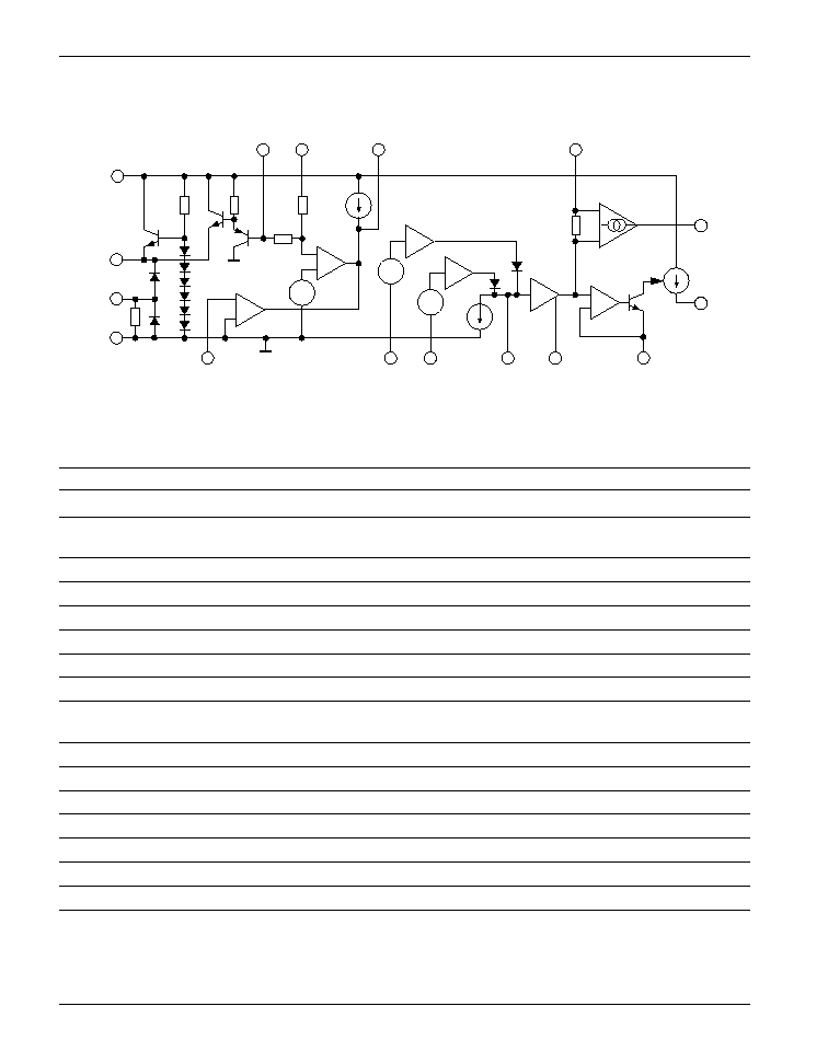
The AS1719D is a 16 pin surface mount IC incorporating the current sense, monitoring, and sharing functions for an
AMPSSTM module. The AS1719D also provides a DC supply voltage for external digital ICs, including an active clamp
to protect the input of a CMOS gate from SCR latchup.
The current sensing circuit provides two channels of current sensing inputs with quasi-peak detection and filtering to a
scaled DC output. This DC output is used to drive a voltage-to-current converter which provides a flexible current
monitor signal which is an output current rather than a voltage.
A differential current share scheme is implemented with a fixed transconductance amplifier. The measured current
from the current sense circuit is compared to and drives a bidirectional input/output pin that represents system current
(SHARE). The result of this comparison is a current source which trims the output voltage of the module to bring it
into equalibrium with other modules in the system.
Description
AS1719D
Current Share Chip
Ordering Information
262
www.ptcc.com.tw
AS1719D
Current Share Chip
VC
VDD
GND
FB
GM = 100
µ
S
MIRR
MON
CLK
DCOK
REGB
REGA
SS
SHAR
CS1
CS2
PK
FLTR
≠
+
≠
+
≠
+
≠
+
≠
+
≠
≠
+
+
100
µ
A
4V
200
µ
A
x5
1k
x1
x1
x1
Block Diagram
Pin Function Description
Pin Number
Function
Description
1
VDD
5V output for driving CMOS circuitry.
2
MON
Voltage output of current sense circuitry - externally loading
this pin creates MIRR current.
3
MIRR
Output current proportional to sensed current.
4
VC
Positive supply input.
5
SHAR
Current share input/output.
6
FB
System feedback node, output of current share amplifier.
7
FLTR
Filter point for reducing noise on current sense signal.
8
GND
Signal ground and silicon substrate.
9
PK
Peak rectifier output - an external cap at this pin creates the
quasi-peak detection scheme.
10
REGA
5.0V voltage reference input.
11
SS
Open collector Soft-start output.
12
DCOK
Sense point for checking (negative) bulk voltage.
13
CS2
Current sense input.
14
CS1
Current sense input.
15
CLK
Clamp for clock signal.
16
REGB
5.0V voltage reference input.
263
www.ptcc.com.tw
AS1719D
Current Share Chip
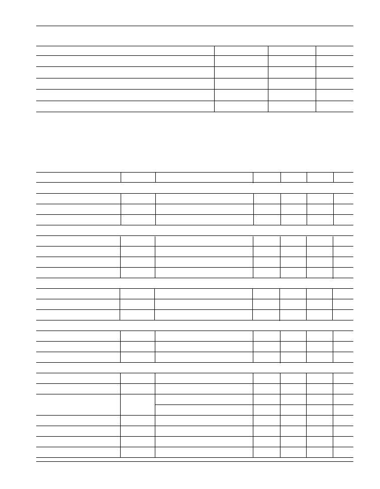
Absolute Maximum Ratings
Parameter
Symbol
Rating
Unit
Supply Voltage
VCC
20
V
Continuous Power
PD
1000
mW
Junction Temperature
TJ
150
∞C
Storage Temperature
TSTG
≠60 to +150
∞C
Lead Temperature (Soldering, 10 seconds)
TL
300
∞C
Electrical Characteristics
Electrical characteristics are guaranteed over the full junction temperature range (-20 -105∞C). Ambient temperature must be der-
ated based upon power dissipation and package thermal characteristics. The conditions are: REGA = 5.0 V; REGB = 5.0 V; 10 V
VC
16V; MIRR = 0 V; FB = 2.5 V; CS1 = 0.5 V; CS2 = 0.5 V; IMON = 100µA; IDD = -10 mA; DCOK = 0 V, unless otherwise
specified.
Parameter
Symbol
Test Condition
Min.
Typ.
Max.
Unit
Bias
Supply Current
IC
IDD = 100µA
5
8.5
14
mA
REGA Current
IREGA
REGB = 0 V
0.2
.5
mA
REGB Current
IREGB
REGA = 0 V
0.1
.5
mA
VDD Regulator
Output Voltage
VDD
IDD = 20 MA
4.7
5
5.4
V
Startup VDD
VDD0
REGA = REGB = 0 V
3.5
4.6
5.5
V
Line Regulation
REGI
8 V
VC
18 V
200
700
mV
Load Regulation
REGO
1 mA
IDD
30 mA
90
400
mV
Soft Start
SS Low Voltage
SSOL
DCOK = 1 V; ISS = 1 mA
0.1
0.4
V
SS Load Current
ISS
SS = 4 V
-100
-155
-210
µA
SS Clamp Voltage
SSOH
5.3
5.6
6
V
Clock Clamp
CLK Positive Clamp
CLKOH
CLK = 500 µA; w/rt VDD
-300
40
300
mV
CLK Negative Clamp
CLKOL
CLK = -500 µA;
-300
40
300
mV
Bleed Resistor
RCLK
ICLK = 10 µA
10
60
k
Current Sense
PK Voltage
VPK
CS1 = 0.5 V; CS2 = 0 V
1.5
1.8
2.2
V
FLTR Voltage
VFLTR
CS1 = 0.5 V; CS2 = 0 V
3.6
4.6
5.2
V
MON Voltage
VMON
CS 1 = 1 V; CS2 = 0 V
4.7
5.0
5.5
V
CS1 = 0 V; CS2 = 1 V
4.7
5.0
5.5
V
MON Gain
AVMON
VMON/
VCS1
4.6
5
5.3
V/V
PK Pull-Down Current
IPK
PK = 2.5 V
125
170
250
µA
CS1 Bias Current
IBCS1
-2
-10
µA
CS2 Bias Current
IBCS2
-2
-10
µA
264
www.ptcc.com.tw
AS1719D
Current Share Chip
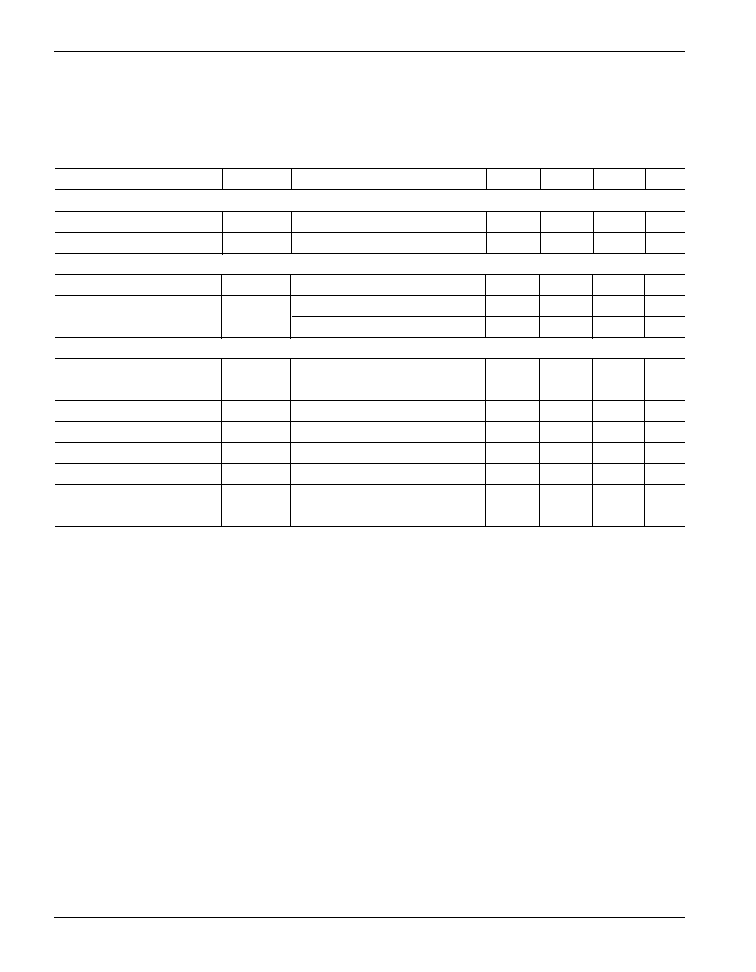
Electrical Characteristics
Electrical characteristics are guaranteed over the full junction temperature range (-20 -105∞C). Ambient temperature must be der-
ated based upon power dissipation and package thermal characteristics. The conditions are: REGA = 5.0 V; REGB = 5.0 V; 10 V
VC
16V; MIRR = 0 V; FB = 2.5 V; CS1 = 0.5 V; CS2 = 0.5 V; IMON = 100µA; IDD = -10 mA; DCOK = 0 V, unless otherwise
specified.
Parameter
Symbol
Test Condition
Min.
Typ.
Max.
Unit
Current Monitor
Mirror Gain
AI
50 µA
IMON
200 µA
195
2.05
2.25
µA/µA
Output Impedance
ZMIRR
0 v
MIRR
5 V
0.5
1
M
DCOK
On Voltage
DCOK
-200
0
200
mV
Hysteresis
DCHY
TJ = 25∞C
500
700
1000
mV
Over Temperature
500
700
1200
mV
Current Share
Transfer Current Gain
AISHR
IFB/
ISHAR;
92
110
125
mA/A
-500 µA
ISHAR
500 µA
Input Impedance
RSHAR
-100 µA
ISHAR
100 µA
0.7
1
1.3
k
Output Impedance
RFB
2 V
FB
3 V; ISHAR = 0
1
m
No-Share Output
IFB
SHAR = 0 µA (Open)
-10
10
µA
SHARE Voltage
VSHAR
CS1 = 0 V; CS2 = 1 V
4.7
5.0
5.5
V
SHARE Disconnect
ISHDIS
SHARE = 4 V; DCOK = 1 V;
-10
10
µA
CS1 = CS2 = 0 V