269
www.ptcc.com.tw
SEMICONDUCTOR
The AS1730 is a 16 pin surface mount IC incorporating the current sense, monitoring, and sharing functions for the
AMPSSTM PFC module. The AS1730 also provides some housekeeping functions for providing a controlled start-up of
the module.
There current sensing circuit provides provides an inverting amplifier with a gain of 20, with a high impedance point
brought out to allow filtering of the signal with an external capacitor. This DC output is used to drive a voltage-to-
current converter which provides a flexible current monitor signal which is an output current rather than a voltage.
A differential current share scheme is implemented with a fixed transconductance amplifier. The measured current
from the current sense circuit drives a bidirectional input/output pin that represents system current (SHARE). Any
current flowing in this pin represents an imbalance between similar modules. This imbalance is measured and a
current proportional to it is fed to the system's main summing junction to compensate. Also flowing to this point is a
small current proportional to the current monitor, which makes the output voltage of the module load dependent (non-
zero output impedance). An additional "droop" circuit allows another externally programmed current to be added to
that point.
Description
AS1730A
PFC Current Share IC
Preliminary Specification
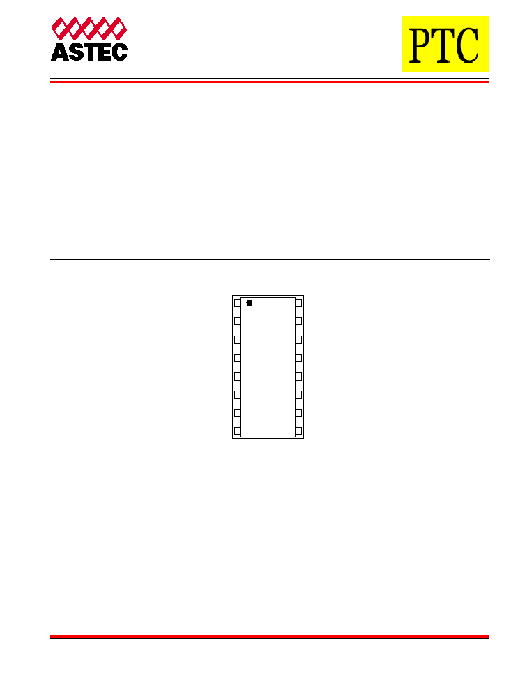
Pin Configuration ≠
Top View
AS1730A
CREF
MON
MIRR
VCC
SHARE
FB
DROOP
GAIN
NMODEN
DCAP
VDD
NCREF
BLKGD
CS
GND
PFW
Ordering Information

271
www.ptcc.com.tw
AS1730A
PFC Current Share IC
Pin Function Description
Pin Number
Function
Description
1
CREF
Input for sensing 7V5 reference from control chip.
2
MON
Voltage output of current sense circuitry - externally loading
this pin creates MIRR current.
3
MIRR
Output current proportional to sensed current.
4
VCC
Positive supply input.
5
SHARE
Current share input/output.
6
FB
System feedback node. Output current is
I
FB
= - + I
DROOP
7
DROOP
Current mirror input (diode to GND) to directly modify FB
output current.
8
GAIN
Filter point for reducing noise on current sense signal.
9
PFW
Power-fall Warning output; open collector NPN. Controlled by
state of BLKGD and DCAP.
10
GND
Signal ground and silicon substrate.
11
CS
Current sense input. Input is expected to be below ground.
12
BLKGD
Logic input (TTL level) controlling PFW output.
13
NCREF
Logic output, saturating NPN with 10k pull-up to VDD.
14
VDD
5 V logic supply input.
15
DCAP
Delay capacitor is discharged in response to NMODEN signal.
16
NMODEN
Logic input (TTL level) controlling DCAP.
I
MON
5
I
SHARE
10
Absolute Maximum Ratings
Parameter
Symbol
Rating
Unit
Supply Voltage
VCC
20
V
Continuous Power
PD
1000
mW
Junction Temperature
TJ
150
∞C
Storage Temperature
TSTG
≠60 to +150
∞C
Lead Temperature (Soldering, 10 seconds)
TL
300
∞C

272
www.ptcc.com.tw
AS1730A
PFC Current Share IC
Electrical Characteristics
Electrical characteristics are guaranteed over the full junction temperature range (-20 -125∞C). Ambient temperature must be der-
ated based upon power dissipation and package thermal characteristics. The conditions are: VDD = 5.0 V; 9 V
VCC
19 V;
MIRR = 0 V; FB = 7V5; CS = -200 mV; MON open; NMODEN = 0 V; BLKGD = 0 V, unless otherwise specified.
Parameter
Symbol
Test Condition
Min.
Typ.
Max.
Unit
Bias
Supply Current
ICC
VCC = 19 V
6
10
mA
VDD Current
IDD
CREF = 7.5 V
0.5
1.5
mA
NCREF Vol
NCROL
CREF = 7.4 V
0.07
0.4
V
NCREF Voh
NCROH
CREF = 5.5 V
4.5
5
V
CREF Bias Current
ICREF
CREF = 8 V
0.3
0.6
mA
DCAP Vol
DCAPOL
NMODEN = 2 V; DCAP = 1 mA
0.02
0.4
V
DCAP Voh
DCAPOH
NMODEN = 0.8 V; DCAP = 100 µA
5.6
6.0
V
NMODEN Bias Current
INMOD
NMODEN = 0 V
30
100
µA
PFW Leakage
PFWLK
PFW = 6V; BLKGD = 2 V; DCAP = 5.2 V
0.01
5
µA
PFW Vol
PFWOL
PFW = 10mA; BLKGD = 0.8V; DCAP= 4..8V
0.1
0.4
V
BLKGD Bias Current
IBLKGD
DCAP = 5.2 V
1
20
µA
GAIN Voltage
VGAIN
CS = -200 mV (Char Data)
4.8
5.3
5.8
V
GAIN Impedance
ZGAIN
I GAIN = 10 µA
36
52
68
k
MON Voltage
VMON0
CS = 0 V; IMON = 250 µA
-0.1
-0.4
0.1
V
VMON
CS = -250 mV (Char Data)
4.6
4.8
5.1
V
MON Gain
AVMON
VMON/
VCS (Char Data)
19.5
V/V
SHARE Voltage
VSHAR0
CS = 0 V
0.02
0.1
V
VSHAR
CS = -250 mV
4.4
5.0
5.0
V
SHARE Gain
AVSHAR
VSHARE/
VCS
19.5
V/V
MIRR Gain
KMIRR
CS = -250 mV; MON = 250µA
0.95
1.05
1.15
mA
MIRR Impedance
ZMIRR
CS = -250 mV; MON = 250µA;
1
m
OV
MIRR
5 V
FB Sense Current
FBCS
CS = -250 mV; MON = -250 µA
-50
-65
-80
µA
Current Share
Transfer Current Gain
KSHARE
IFB/
ISHAR; 500 µA
ISHAR
500 µA
95
100
105
mA/A
Input Impedance
RSHARE
100 µA
ISHAR
100 µA
0.7
1
1.3
k
Output Impedance
RFB
2 V
FB
3 V; ISHAR = 0
1
3
m
No-Share Output
IFB
SHARE Open; MON Open
-15
-5
5
µA
