 | –≠–ª–µ–∫—Ç—Ä–æ–Ω–Ω—ã–π –∫–æ–º–ø–æ–Ω–µ–Ω—Ç: AS1731 | –°–∫–∞—á–∞—Ç—å:  PDF PDF  ZIP ZIP |
281
www.ptcc.com.tw
SEMICONDUCTOR
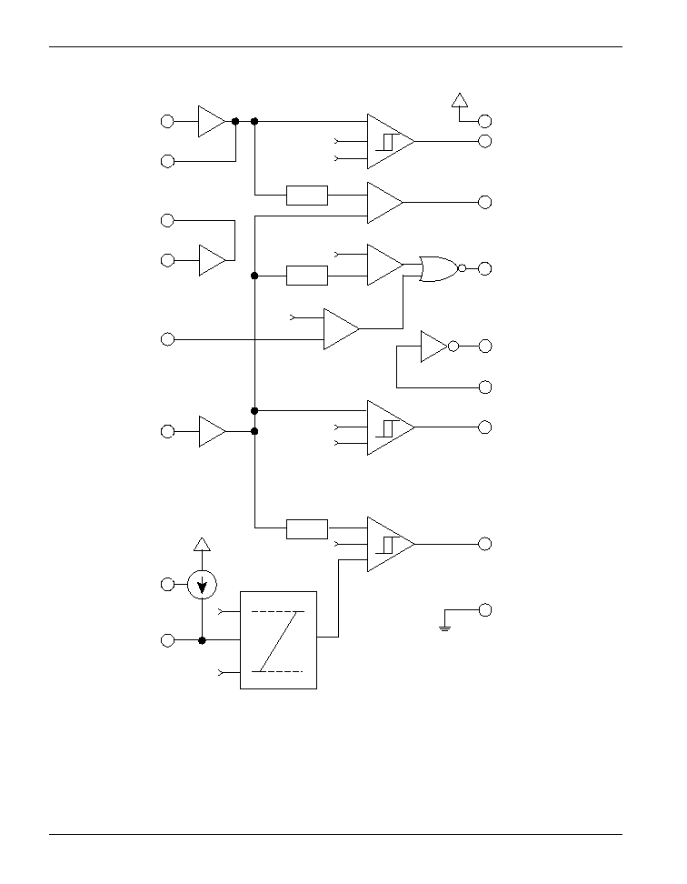
The AS1731 is a 18 pin surface mount IC incorporating input and output voltage monitoring for the AMPSSTM PFC
module. The AS1731 also provides some housekeeping functions for providing a controlled start-up of the module.
External dividers bring in analogs of the peak AC input (VPK) and the PFC output (VBLK). These signals are
buffered and compared to a fixed reference to control startup and shutdown sequencing and to report faults.
Description
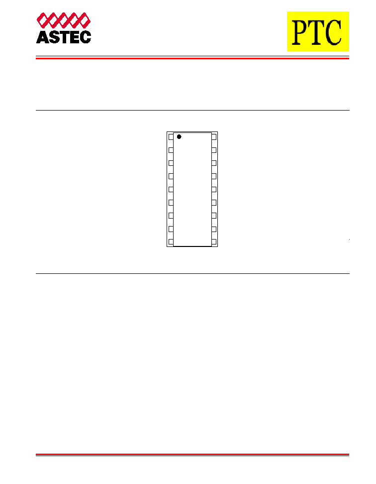
Pin Configuration ≠
Top View
AS1731B
TEMP
OVP
MODEN
NMODEN
BLKOK
BLKGD
PFWADJ
CSET
VDD2
VCC
VDD
REF
INRDY
KVPK
PKSNS
PKVO
GND
BLKSNS
AS1731B
PFC Monitoring IC
Preliminary Specification
Ordering Information
282
www.ptcc.com.tw
AS1731B
PFC Monitoring IC
+
-
-
+
+
+
+
-
-
-
-
-
+
-
-
x1
x1
x2
VDD
3V55
3V65
4V1
5V
3V5
2V5
1V7
x 0.875
3V85
PKSNS
KVPK
VDD
REF
TEMP
BLKSNS
CSET
PFWADJ
INRDY
VCC
PKVO
OVP
MODEN
NMODEN
BLKOK
BLKGD
GND
2V05
x 0.513
x 0.60
LIMITTER
Block Diagram

283
www.ptcc.com.tw
AS1731B
PFC Monitoring IC
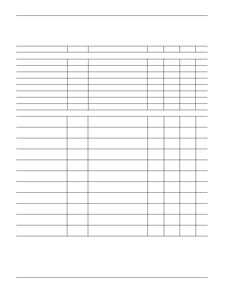
Pin Function Description
Pin Number
Function
Description
1
TEMP
Input from temperature sensor (AS300).
2
OVP
Open collector digital output. Low when VBLK exceeds OV
limit or TEMP exceeds OT limit.
3
MODEN
Open collector digital output; inversion of NMODEN.
4
NMODEN
Logic input (TTL compatible thresholds.)
5
BLKOK
Digital output; active low with 10k pullup to VDD. Low when
VBLK below normal regulation limits.
6
BLKGD
Digital output; active low with 10k pullup to VDD. Low when
BVLK is above the threshold controlled by PFWADJ.
7
PFWADJ
Input sets lower hysteresis point for BLKGD comparator. A
1mA current source (set by CSET) allows ALP
TM
programming.
8
CSET
Buffered 2.5 V output. Load resistor to ground programs cur-
rent for PFWADJ pin.
9
VDD2
5 V supply input (short this pin to VDD.)
10
BLKSNS
Input to VPK buffer.
11
GND
Signal ground and silicon substrate.
12
PKVO
Digital output; active low with 8k pullup to VDD. Low when
VBLK is low with respect to VPK.
13
PKSNS
Input to VPK buffer.
14
KVPK
Output to VPK buffer.
15
INRDY
Digital output; active low with 10k pullup to VDD. Low when
VPK is insufficient to run supply.
16
REF
Input for 2.50 V reference.
17
VDD
Digital (5 V) supply regulator output.
18
VCC
Analog supply voltage.
Absolute Maximum Ratings
Parameter
Symbol
Rating
Unit
Supply Voltage
V
CC
20
V
Continuous Power
P
D
1000
mW
Junction Temperature
T
J
150
∞C
Storage Temperature
T
STG
≠60 to +150
∞C
Lead Temperature (Soldering, 10 seconds)
T
L
300
∞C
284
www.ptcc.com.tw
AS1731B
PFC Monitoring IC
Electrical Characteristics
Electrical characteristics are guaranteed over the full junction temperature range (-20 -125∞C). Ambient temperature must be der-
ated based upon power dissipation and package thermal characteristics. The conditions are: 11 V
VCC
19 V, REF = 2.5 V;
BLKSNS = 6 V; PKSNS = 6 V; TEMP = 3 V; NMODEN = 0 V; CSET = 2k5 to GND, unless otherwise specified.
Parameter
Symbol
Test Condition
Min.
Typ.
Max.
Unit
Bias
Supply Current
ICC
VCC = 19 V
5
10
mA
VDD Voltage
VDD
0
IDD
20 mA
4.5
5
5.5
V
REF Bias Current
REFIB
0
2
µA
TEMP Bias Current
ITMP
1
6
µA
CSET Voltage
VCSET
2.5
V
PFWADJ Current
IPFW
PFWADJ = 3 V
1
mA
PFWADJ Compliance
VPFW
3.65
V
PFWADJ Impedance
ZPFW
OV
PFWADJ
3 V
1
m
Comparator Thresholds
PKSNS Upper Threshold
INRDVIH
2.5
V
for INRDY
PKSNS Lower Threshold
INRDVIL
1.7
V
for INRDY
PKSNS Threshold
PKVVIH
BLKSNS = 5 V
5.71
V
for PKVO
BLKSNS Threshold
OVPVIH
8.33
V
for OVP
TEMP Threshold
TMPVOL
3.85
V
for OVP
BLKSNS Upper Threshold
BLKKVIH
4.1
V
for BLKOK
BLKSNS Lpper Threshold
BLKKVIL
3.5
V
for BLKOK
BLKSNS Upper Threshold
BLKGVIH
7.12
V
for BLKGD
Max. PFWADJ Threshold
PFWMAX
PFWADJ = 4 V
6.92
V
for BLKGD
Nom. PFWADJ Threshold
PFWNOM
PFWADJ = 3 V
5.85
V
for BLKGD
Min. PFWADJ Threshold
PFWMIN
PFWADJ = 1.5 V
4.00
V
for BLKGD

285
www.ptcc.com.tw
AS173B
PFC Monitoring IC
Electrical Characteristics
Electrical characteristics are guaranteed over the full junction temperature range (-20 -125∞C). Ambient temperature must be der-
ated based upon power dissipation and package thermal characteristics. The conditions are: 11 V
VCC
19 V, REF = 2.5 V;
BLKSNS = 6 V; PKSNS = 6 V; TEMP = 3 V; NMODEN = 0 V; CSET = 2k5 to GND, unless otherwise specified.
Parameter
Symbol
Test Condition
Min.
Typ.
Max.
Unit
Buffers
KVBLK Offset
1
VOSBLK
BLKSNS = 3 V; VCC = 15
10
mV
KVBLK Common Mode Error
1
CMRBLK
Vos for 2 V
BLKSNS
12 V;
5
15
mV
VCC = 15 V
KVBLK Power Supply Rejection
1
PSRBLK
Vos for 9 V
VCC
19 V;
5
15
mV
BLKSNS = 5 V
KVBLK Load Reg
1
LRBLK
Vos for = -100 µA
2
5
mV
BLKSNS
100 µA
BLKSNS Bias Current
IBBLK
.5
1.5
µA
KVPK Offset
VOSPK
PKSNS = 3 V
10
mV
KVPK Common Mode Error
CMPRK
Vos for = 2 V
PKSNS
5
15
mV
12V; VCC = 15 V
KVPK Power Supply Rej.
PSRPK
Vos for = 9 V
VCC
5
15
mV
19 V; PKSNS = 5 V
KVPK Load Reg.
LRPK
- 100 µA
PKSNS
100 µA
2
5
mV
PKSNS Bias Current
IBPK
.5
1.5
µA
Logic
MODEN Output Low
MODVOL
VMODEN = 2 V; MODEN = 1 mA
0.1
0.4
V
MODEN Leakage
MODLKG
NMODEN = 0.8 V; MODEN = 6 V
.01
5
µA
NMODEN Bias Current
NMODIB
NMODEN = 0.8 V
-50
-10
µA
INRDY Low Output
INRDVOL
PKSNS = 1.6; INRDY = 1 mA
0.2
0.4
V
INRDY High Output
INRDVOH
PKSNS = 2.6; INRDY = . 1mA
3.5
V
PKVO Low Output
PKVVOL
BLKSNS = 5 V; PKVO = 1 mA
0.2
0.4
V
PKVO High Output
PKVVOH
PKVO = -100 µA
3.5
V
OVP Low Output
OVPVOL
BLKSNS = 8.5 V; OVP = 1 mA
0.2
0.4
V
OVP Leakage
OVPLKG
OVP = 6 V
.01
5
µA
BLKOK Low Output
BLKKVOL
BLKSNS = 3 V; BLKOK = 1 mA
0.2
0.4
V
BLKOK High Output
BLKKVOH
BLKOK = -100 µA
3.5
V
BLKGD Low Output
BLKGVOL
BLKSNS = 2 V; BLKGD = 1 mA
0.2
0.4
V
BLKGD High Output
BLKGVOH
BLKGD = -100 µA
4.5
V
Note 1: These parameters are verified at water test and cannot be tested in packaged form.