 | –≠–ª–µ–∫—Ç—Ä–æ–Ω–Ω—ã–π –∫–æ–º–ø–æ–Ω–µ–Ω—Ç: 45DB011B | –°–∫–∞—á–∞—Ç—å:  PDF PDF  ZIP ZIP |

1
1-Megabit
2.7-volt Only
Serial
DataFlash
Æ
AT45DB011
Preliminary
Features
∑
Single 2.7V - 3.6V Supply
∑
Serial Interface Architecture
∑
Page Program Operation
≠ Single Cycle Reprogram (Erase and Program)
≠ 512 Pages (264 Bytes/Page) Main Memory
∑
Optional Page and Block Erase Operations
∑
One 264-Byte SRAM Data Buffer
∑
Internal Program and Control Timer
∑
Fast Page Program Time ≠ 7 ms Typical
∑
120
µ
s Typical Page to Buffer Transfer Time
∑
Low-Power Dissipation
≠ 4 mA Active Read Current Typical
≠ 2
µ
A CMOS Standby Current Typical
∑
13 MHz Max Clock Frequency
∑
Hardware Data Protection Feature
∑
Serial Peripheral Interface (SPI) Compatible ≠ Modes 0 and 3
∑
CMOS and TTL Compatible Inputs and Outputs
∑
Commercial and Industrial Temperature Ranges
Description
The AT45DB011 is a 2.7-volt only, serial interface Flash memory suitable for in-sys-
tem reprogramming. Its 1,081,344 bits of memory are organized as 512 pages of 264
bytes each. In addition to the main memory, the AT45DB011 also contains one SRAM
data buffer of 264 bytes. Unlike conventional Flash memories that are accessed ran-
domly with multiple address lines and a parallel interface, the DataFlash uses a serial
interface to sequentially access its data. The simple serial interface facilitates hard-
Rev. 1103C≠08/98
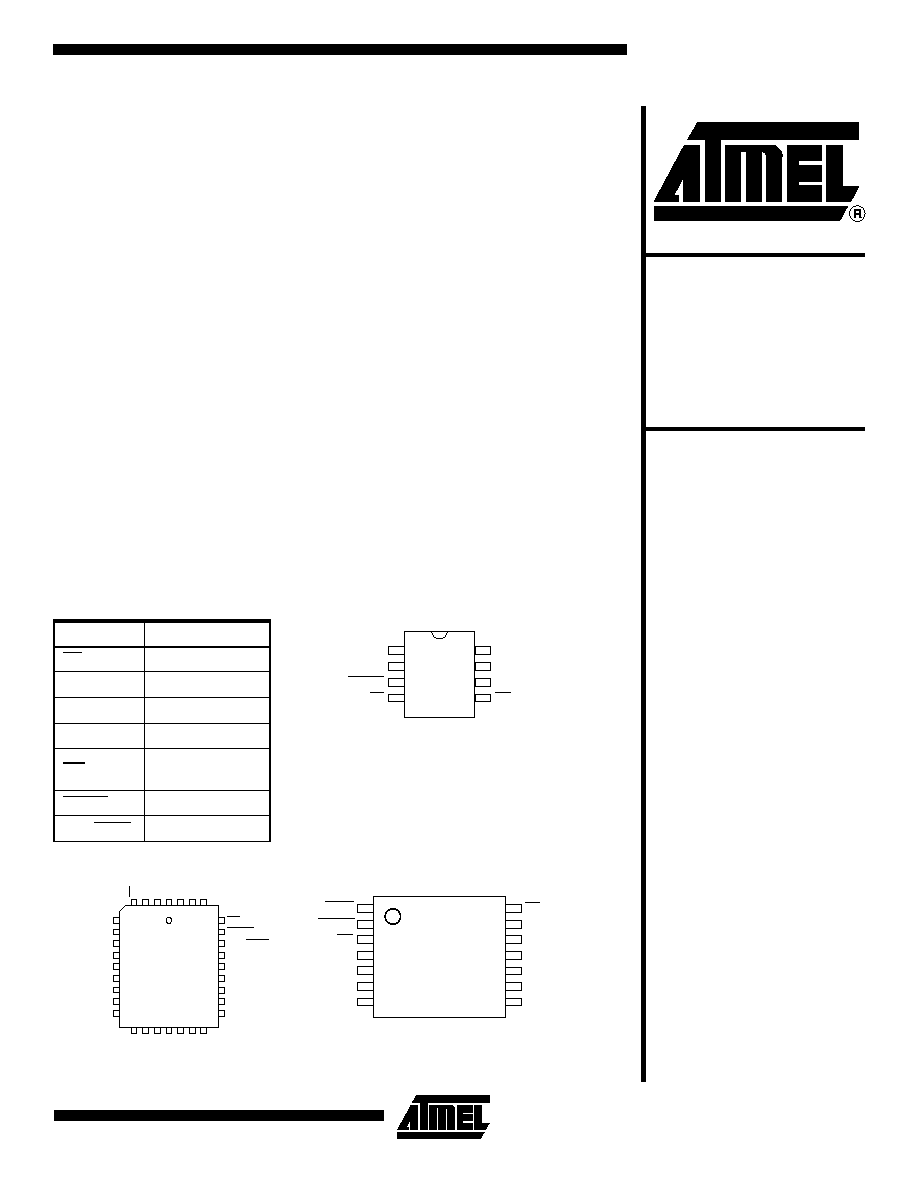
Pin Configurations
Pin Name
Function
CS
Chip Select
SCK
Serial Clock
SI
Serial Input
SO
Serial Output
WP
Hardware Page
Write Protect Pin
RESET
Chip Reset
RDY/BUSY
Ready/Busy
(continued)
TSSOP Top View
Type 1
1
2
3
4
5
6
7
14
13
12
11
10
9
8
RDY/BUSY
RESET
WP
VCC
GND
SCK
SO
CS
NC
NC
NC
NC
NC
SI
PLCC
5
6
7
8
9
10
11
12
13
29
28
27
26
25
24
23
22
21
SCK
SI
SO
NC
NC
NC
NC
NC
NC
WP
RESET
RDY/BUSY
NC
NC
NC
NC
NC
NC
4
3
2
1
32
31
30
14
15
16
17
18
19
20
NC
NC
DC
DC
NC
NC
NC
CS
NC
NC
GND
VCC
NC
NC
SOIC
1
2
3
4
8
7
6
5
SI
SCK
RESET
CS
SO
GND
VCC
WP
Note: PLCC package pins 16
and 17 are DON'T CONNECT
AT45DB011
Preliminary 16-
Megabit 2.7-volt
Only Serial
DataFlash

AT45DB011
2
ware layout, increases system reliability, minimizes switch-
ing noise, and reduces package size and active pin count.
The device is optimized for use in many commercial and
industrial applications where high density, low pin count,
low voltage, and low power are essential. Typical applica-
tions for the DataFlash are digital voice storage, image
storage, and data storage. The device operates at clock
frequencies up to 13 MHz with a typical active read current
consumption of 4 mA.
To allow for simple in-system reprogrammability, the
AT45DB011 does not require high input voltages for pro-
gramming. The device operates from a single power sup-
p ly , 2 . 7 V t o 3 . 6 V , f o r b o t h t h e p r o g r a m a n d r e a d
operations. The AT45DB011 is enabled through the chip
select pin (CS) and accessed via a three-wire interface
consisting of the Serial Input (SI), Serial Output (SO), and
the Serial Clock (SCK).
All programming cycles are self-timed, and no separate
erase cycle is required before programming.
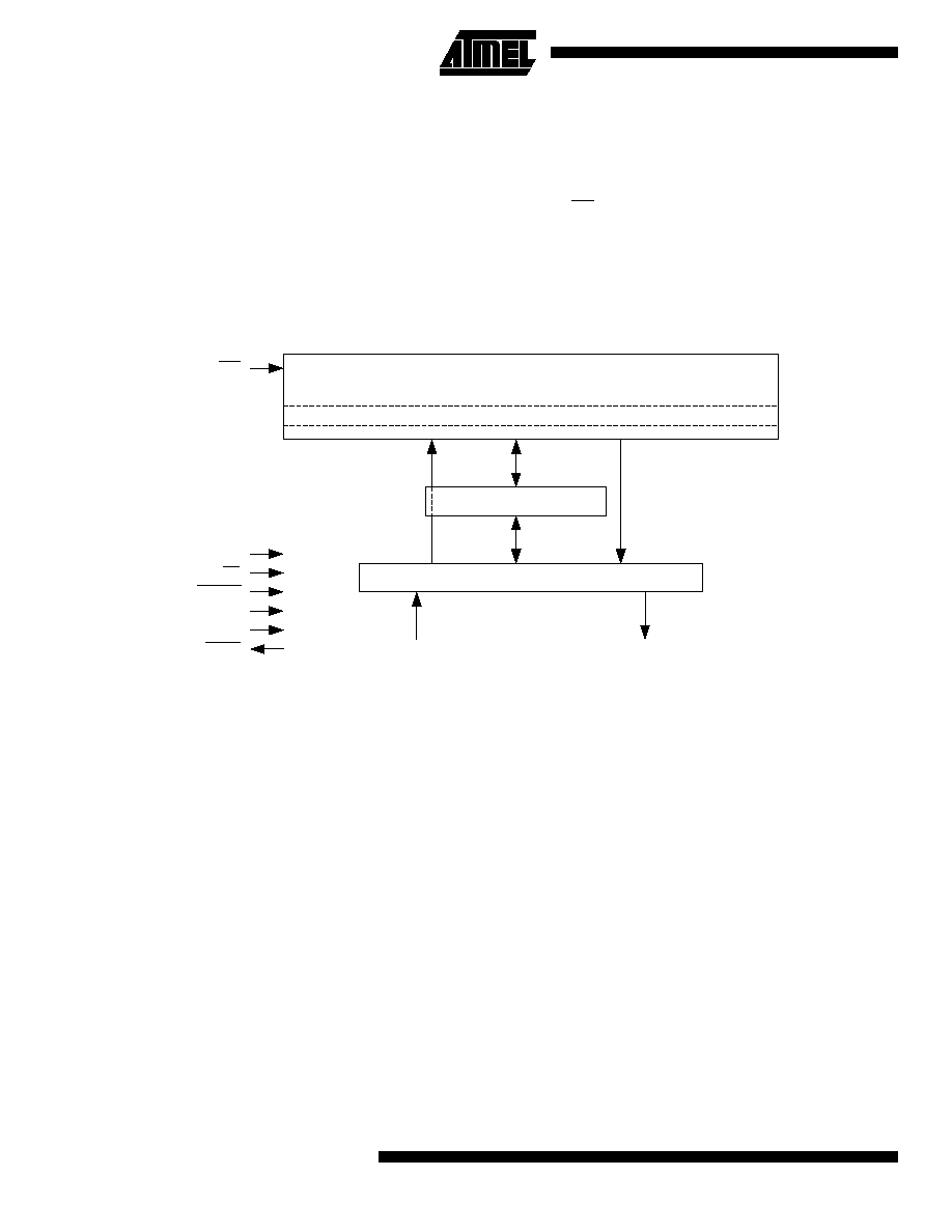
Block Diagram
Memory Array
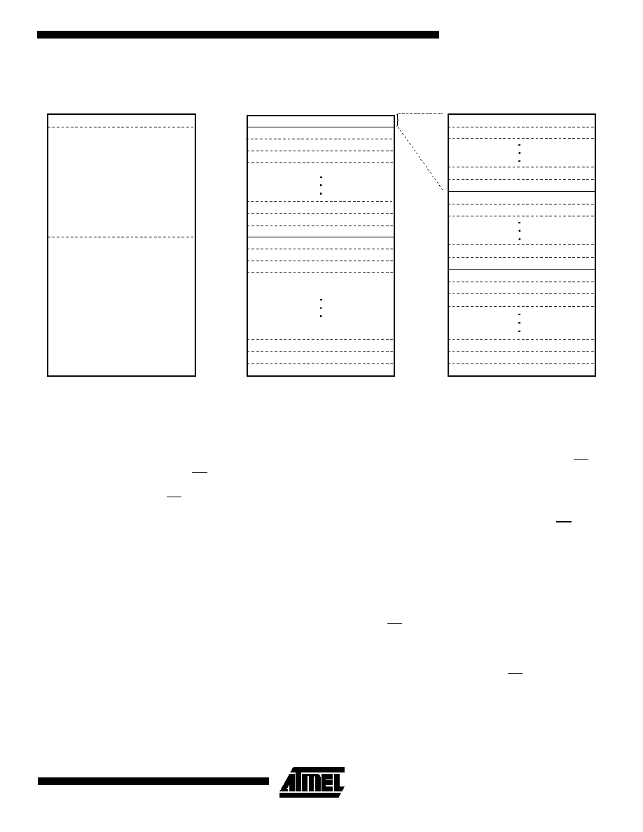
To provide optimal flexibility, the memory array of the
AT45DB011 is divided into three levels of granularity com-
prising of sectors, blocks, and pages. The Memory Archi-
tecture Diagram illustrates the breakdown of each level and
details the number of pages per sector and block. All pro-
gram operations to the DataFlash occur on a page by page
basis; however, the optional erase operations can be per-
formed at the block or page level.
FLASH MEMORY ARRAY
PAGE (264 BYTES)
BUFFER (264 BYTES)
I/O INTERFACE
SCK
CS
RESET
V
CC
GND
RDY/BUSY
WP
SO
SI

AT45DB011
3
Memory Architecture Diagram
Device Operation
The device operation is controlled by instructions from the
host processor. The list of instructions and their associated
opcodes are contained in Tables 1 and 2. A valid instruc-
tion starts with the falling edge of CS followed by the appro-
priate 8-bit opcode and the desired buffer or main memory
address location. While the CS pin is low, toggling the SCK
pin controls the loading of the opcode and the desired
buffer or main memory address location through the SI
(serial input) pin. All instructions, addresses, and data are
transferred with the most significant bit (MSB) first.
Read
By specifying the appropriate opcode, data can be read
from the main memory or from the data buffer.
MAIN MEMORY PAGE READ: A main memory read allows
the user to read data directly from any one of the 512
pages in the main memory, bypassing the data buffer and
leaving the contents of the buffer unchanged. To start a
page read, the 8-bit opcode, 52H, is followed by 24
address bits and 32 don't care bits. In the AT45DB011, the
first six address bits are reserved for larger density devices
(see Notes on page 9), the next nine address bits (PA8-
PA0) specify the page address, and the next nine address
bits (BA8-BA0) specify the starting byte address within the
page. The 32 don't care bits which follow the 24 address
bits are sent to initialize the read operation. Following the
32 don't care bits, additional pulses on SCK result in serial
data being output on the SO (serial output) pin. The CS pin
must remain low during the loading of the opcode, the
address bits, and the reading of data. When the end of a
page in main memory is reached during a main memory
page read, the device will continue reading at the beginning
of the same page. A low to high transition on the CS pin will
terminate the read operation and tri-state the SO pin.
BUFFER READ: Data can be read from the data buffer
using an opcode of 54H. To perform a buffer read, the eight
bits of the opcode must be followed by 15 don't care bits,
nine address bits, and eight don't care bits. Since the buffer
size is 264-bytes, nine address bits (BFA8-BFA0) are
required to specify the first byte of data to be read from the
buffer. The CS pin must remain low during the loading of
the opcode, the address bits, the don't care bits, and the
reading of data. When the end of the buffer is reached, the
device will continue reading back at the beginning of the
buffer. A low to high transition on the CS pin will terminate
the read operation and tri-state the SO pin.
MAIN MEMORY PAGE TO BUFFER TRANSFER: A page
of data can be transferred from the main memory to buffer.
An 8-bit opcode of 53H is followed by the six reserved bits,
nine address bits (PA8-PA0) which specify the page in
Block = 2112 bytes
(2K + 64)
8 Pages
BLOCK 0
BLOCK 1
BLOCK 2
BLOCK 62
BLOCK 63
BLOCK 61
Page = 264 bytes
(256 + 8)
PAGE 0
PAGE 1
PAGE 6
PAGE 7
PAGE 8
PAGE 9
PAGE 510
PAGE 511
BLOCK 0
PAGE 14
PAGE 15
PAGE 16
PAGE 17
PAGE 18
PAGE 509
BLOCK 1
BLOCK ARCHITECTURE
PAGE ARCHITECTURE
SECTOR 0 = 2112 BYTES (2K + 64)
SECTOR 1 = 65,472 BYTES (62K + 1984)
SECTOR ARCHITECTURE
SECTOR 2 = 67,584 BYTES (64K + 2K)
BLOCK 3
BLOCK 29
BLOCK 30
BLOCK 31
BLOCK 32
BLOCK 33
BLOCK 34
SECTOR 1
SECTOR 2
SECTOR 0

AT45DB011
4
main memory that is to be transferred, and nine don't care
bits. The CS pin must be low while toggling the SCK pin to
load the opcode, the address bits, and the don't care bits
from the SI pin. The transfer of the page of data from the
main memory to the buffer will begin when the CS pin tran-
sitions from a low to a high state. During the transfer of a
page of data (t
XFR
), the status register can be read to deter-
mine whether the transfer has been completed or not.
MAIN MEMORY PAGE TO BUFFER COMPARE: A page of
data in main memory can be compared to the data in the
buffer. An 8-bit opcode of 60H is followed by 24 address
bits consisting of the six reserved bits, nine address bits
(PA8-PA0) which specify the page in the main memory that
is to be compared to the buffer, and nine don't care bits.
The loading of the opcode and the address bits is the same
as described previously. The CS pin must be low while tog-
gling the SCK pin to load the opcode, the address bits, and
the don't care bits from the SI pin. On the low to high transi-
tion of the CS pin, the 264 bytes in the selected main mem-
ory page will be compared with the 264 bytes in the buffer.
During this time (t
XFR
), the status register will indicate that
the part is busy. On completion of the compare operation,
bit 6 of the status register is updated with the result of the
compare.
Program
BUFFER WRITE: Data can be shifted in from the SI pin
into the data buffer. To load data into the buffer, an 8-bit
opcode of 84H is followed by 15 don't care bits and nine
address bits (BFA8-BFA0). The nine address bits specify
the first byte in the buffer to be written. The data is entered
following the address bits. If the end of the data buffer is
reached, the device will wrap around back to the beginning
of the buffer. Data will continue to be loaded into the buffer
until a low to high transition is detected on the CS pin.
BUFFER TO MAIN MEMORY PAGE PROGRAM WITH
BUILT-IN ERASE: Data written into the buffer can be pro-
grammed into the main memory. An 8-bit opcode of 83H is
followed by the six reserved bits, nine address bits (PA8-
PA0) that specify the page in the main memory to be writ-
ten, and nine additional don't care bits. When a low to high
transition occurs on the CS pin, the part will first erase the
selected page in main memory to all 1s and then program
the data stored in the buffer into the specified page in the
main memory. Both the erase and the programming of the
page are internally self timed and should take place in a
maximum time of t
EP
. During this time, the status register
will indicate that the part is busy.
BUFFER TO MAIN MEMORY PAGE PROGRAM WITH-
OUT BUILT-IN ERASE: A previously erased page within
main memory can be programmed with the contents of the
buffer. An 8-bit opcode of 88H is followed by the six
reserved bits, nine address bits (PA8-PA0) that specify the
page in the main memory to be written, and nine additional
don't care bits. When a low to high transition occurs on the
CS pin, the part will program the data stored in the buffer
into the specified page in the main memory. It is necessary
that the page in main memory that is being programmed
has been previously erased. The programming of the page
is internally self timed and should take place in a maximum
time of t
P
. During this time, the status register will indicate
that the part is busy.
PAGE ERASE: The optional Page Erase command can be
used to individually erase any page in the main memory
array allowing the Buffer to Main Memory Page Program
without Built-In Erase command to be utilized at a later
time. To perform a Page Erase, an opcode of 81H must be
loaded into the device, followed by six reserved bits, nine
address bits (PA8-PA0), and nine don't care bits. The nine
address bits are used to specify which page of the memory
array is to be erased. When a low to high transition occurs
on the CS pin, the part will erase the selected page to 1s.
The erase operation is internally self-timed and should take
place in a maximum time of t
PE
. During this time, the status
register will indicate that the part is busy.
BLOCK ERASE: A block of eight pages can be erased at
one time allowing the Buffer to Main Memory Page Pro-
gram without Built-In Erase command to be utilized to
reduce programming times when writing large amounts of
data to the device. To perform a Block Erase, an opcode of
50H must be loaded into the device, followed by six
reserved bits, six address bits (PA8-PA3), and 12 don't
care bits. The six address bits are used to specify which
block of eight pages is to be erased. When a low to high
transition occurs on the CS pin, the part will erase the
selected block of eight pages to 1s. The erase operation is
internally self-timed and should take place in a maximum
time of t
BE
. During this time, the status register will indicate
that the part is busy.

AT45DB011
5
MAIN MEMORY PAGE PROGRAM: This operation is a
combination of the Buffer Write and Buffer to Main Memory
Page Program with Built-In Erase operations. Data is first
shifted into the buffer from the SI pin and then programmed
into a specified page in the main memory. An 8-bit opcode
of 82H is followed by the six reserved bits and 18 address
bits. The nine most significant address bits (PA8-PA0)
select the page in the main memory where data is to be
written, and the next nine address bits (BFA8-BFA0) select
the first byte in the buffer to be written. After all address bits
are shifted in, the part will take data from the SI pin and
store it in the data buffer. If the end of the buffer is reached,
the device will wrap around back to the beginning of the
buffer. When there is a low to high transition on the CS pin,
the part will first erase the selected page in main memory to
all 1s and then program the data stored in the buffer into
the specified page in the main memory. Both the erase and
the programming of the page are internally self timed and
should take place in a maximum of time t
EP
. During this
time, the status register will indicate that the part is busy.
AUTO PAGE REWRITE: This mode is only needed if multi-
ple bytes within a page or multiple pages of data are modi-
fied in a random fashion. This mode is a combination of two
operations: Main Memory Page to Buffer Transfer and
Buffer to Main Memory Page Program with Built-In Erase.
A page of data is first transferred from the main memory to
the data buffer, and then the same data (from the buffer) is
programmed back into its original page of main memory.
An 8-bit opcode of 58H is followed by the six reserved bits,
nine address bits (PA8-PA0) that specify the page in main
memory to be rewritten, and nine additional don't care bits.
When a low to high transition occurs on the CS pin, the part
will first transfer data from the page in main memory to the
buffer and then program the data from the buffer back into
same page of main memory. The operation is internally
self-timed and should take place in a maximum time of t
EP
.
During this time, the status register will indicate that the
part is busy.
If a sector is programmed or reprogrammed sequentially
page by page, then the programming algorithm shown in
Figure 1 is recommended. Otherwise, if multiple bytes in a
page or several pages are programmed randomly in a sec-
tor, then the programming algorithm shown in Figure 2 is
recommended.
STATUS REGISTER: The status register can be used to
determine the device's ready/busy status, the result of a
Main Memory Page to Buffer Compare operation, or the
device density. To read the status register, an opcode of
57H must be loaded into the device. After the last bit of the
opcode is shifted in, the eight bits of the status register,
starting with the MSB (bit 7), will be shifted out on the SO
pin during the next eight clock cycles. The five most-signifi-
cant bits of the status register will contain device informa-
tion, while the remaining three least-significant bits are
reserved for future use and will have undefined values.
After bit 0 of the status register has been shifted out, the
sequence will repeat itself (as long as CS remains low and
SCK is being toggled) starting again with bit 7. The data in
the status register is constantly updated, so each repeating
sequence will output new data.
Ready/busy status is indicated using bit 7 of the status reg-
ister. If bit 7 is a 1, then the device is not busy and is ready
to accept the next command. If bit 7 is a 0, then the device
is in a busy state. The user can continuously poll bit 7 of the
status register by stopping SCK once bit 7 has been output.
The status of bit 7 will continue to be output on the SO pin,
and once the device is no longer busy, the state of SO will
change from 0 to 1. There are eight operations which can
cause the device to be in a busy state: Main Memory Page
to Buffer Transfer, Main Memory Page to Buffer Compare,
Block Erase Addressing
PA8
PA7
PA6
PA5
PA4
PA3
PA2
PA1
PA0
Block
0
0
0
0
0
0
X
X
X
0
0
0
0
0
0
1
X
X
X
1
0
0
0
0
1
0
X
X
X
2
0
0
0
0
1
1
X
X
X
3
∑
∑
∑
∑
∑
∑
∑
∑
∑
∑
∑
∑
∑
∑
∑
∑
∑
∑
∑
∑
∑
∑
∑
∑
∑
∑
∑
∑
∑
∑
1
1
1
1
0
0
X
X
X
60
1
1
1
1
0
1
X
X
X
61
1
1
1
1
1
0
X
X
X
62
1
1
1
1
1
1
X
X
X
63
