1
Features
∑
32-bit RISC Architecture
∑
Two Instruction Sets:
≠ ARM
Æ
High-performance 32-bit Instruction Set
≠ Thumb
Æ
High-code-density 16-bit Instruction Set
∑
Very Low Power Consumption: Industry-leader in MIPS/Watt
∑
4G Bytes Linear Address Space
∑
Von Neumann Load/Store Architecture:
≠ Single 32-bit Data Bus for Instructions and Data
∑
3-Stage Pipeline Architecture:
≠ Fetch, Decode and Execute Stage
∑
8-, 16-, and 32-bit Data Types
∑
Single Cycle 32x8 Hardware Multiplier:
≠ Multiplication is Accelerated when Upper Bytes Are All Zero or One
∑
On-chip JTAG Debug and In Circuit Emulation
∑
Extensive Range of Third-party Application Development Tools
Description
The ARM7TDMITM embedded microcontroller core is a member of the Advanced
RISC Machines (ARM
Æ
) family of general purpose 32-bit microprocessors, which offer
high performance and very lower power consumption. Its outstanding feature is the
16-bit Thumb
Æ
subset of the most commonly used 32-bit instructions. These are
expanded at run time with no degradation of system performance. This gives 16-bit
code density (saving memory area and cost) coupled with 32-bit processor
performance.
The ARM architecture is based on Reduced Instruction Set Computer (RISC) princi-
ples, and the instruction set and related decode mechanism are much simpler than
those of microprogrammed Complex Instruction Set Computers. This simplicity results
in a high instruction throughput and impressive real-time interrupt response from a
small and cost-effective chip.
Pipelining is employed so that all parts of the processing and memory systems can
operate continuously. Typically, while one instruction is being executed, its successor
is being decoded, and a third instruction is being fetched from memory.
The ARM memory interface has been designed to allow the performance potential to
be realized without incurring high costs in the memory system. Speed-critical control
signals are pipelined to allow system control functions to be implemented in standard
low-power logic, and these control signals facilitate the exploitation of the fast local
access modes offered by industry standard dynamic RAMs.
The ARM memory interface is also ideally suited to interfacing, either on-chip or off-
chip, with Atmel's Flash memory blocks. These give the benefits of in-system pro-
grammability and security, reducing time-to-market and system cost.
The ARM7TDMI core is supported by an extensive range of application development
tools. These are fully described in the AT91Business Partners section of Atmels's
Web site (www.atmel.com).
Embedded RISC
Microcontroller
Core
ARM7TDMITM
Rev. 0673CS≠11/99
Note: This is a summary document. For the complete 204-page
document, please visit our web site at www.atmel.com or e-mail at
literature@atmel.com and request literature #0673B.

ARM7TDMI
4
ARM7TDMI Processor
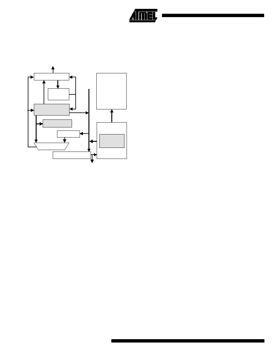
Figure 3. ARM7TDMI Processor
The ARM7TDMI processor is built around a bank of 37 32-
bit registers and six status registers. It features an integral
32 x 8 multiplier and 32-bit barrel shifter. Five independent
internal buses (the PC Bus, the Increment Bus, the ALU
Bus and the A- and B-Buses) allow a high degree of paral-
lelism in instruction execution.
Operating Modes
ARM7TDMI supports seven modes of operation:
∑ User (usr):
The normal ARM program execution state
∑ FIQ (fiq):
Designed to support a data transfer or channel process
∑ IRQ (irq):
Used for general-purpose interrupt handling
∑ Supervisor (svc):
Protected mode for the operating system
∑ Abort mode (abt):
Entered after a data or instruction prefetch abort
∑ System (sys):
A privileged user mode for the operating system
∑ Undefined (und):
Entered when an undefined instruction is executed
Mode changes may be made under software control, or
may be brought about by external interrupts or exception
processing. Most application programs will execute in User
mode. The non-user modes - known as privileged modes -
are entered in order to service interrupts or exceptions, or
to access protected resources.
Each operating mode has dedicated banked registers for
fast exception handling. The FIQ mode has five additional
banked working registers, r8_fiq to r12_fiq, to enhance
interrupt processing speed.
Address Register
37 32-bit Registers
(including 6 status registers)
Address
Incrementer
32 x 8 Multiplier
Barrel Shifter
32-bit ALU
Write Data Register
ARM
Instruction Decoder
&
Control Logic
Instruction
Thumb
Instruction
Decompressor
Pipeline
32-Bit Address Bus
32-bit Data Bus
PC
Bus
A-B
u
s
B-B
u
s
Increment Bus
AL
U Bus

ARM7TDMI
5
Registers
ARM7TDMI has a total of 37 registers ≠ 31 general-pur-
pose 32-bit registers and six status registers ≠ but these
cannot all be seen at once. The processor state and oper-
ating mode dictate which registers are available to the pro-
grammer.
The ARM State Register Set
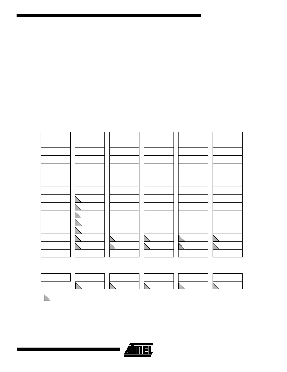
In ARM state, 16 general registers and one or two status
registers are visible at any one time. In privileged (non-
User) modes, mode-specific banked registers are switched
in. Figure 4 shows which registers are available in each
mode: the banked registers are marked with a shaded tri-
angle.
The ARM state register set contains 16 directly accessible
registers: R0 to R15. All of these except R15 are general-
purpose, and may be used to hold either data or address
values. In addition to these, there is a seventeenth register
used to store status information.
Figure 4. Register Organization in ARM State
ARM State General Registers and Program Counter
R0
R1
R2
R3
R4
R5
R6
R7
R8
R9
R10
R11
R12
R13
R14
R15 (PC)
R0
R1
R2
R3
R4
R5
R6
R7
R8_fiq
R9_fiq
R10_fiq
R11_fiq
R12_fiq
R13_fiq
R14_fiq
R15 (PC)
R0
R1
R2
R3
R4
R5
R6
R7
R8
R9
R10
R11
R12
R13_svc
R14_svc
R15 (PC)
R0
R1
R2
R3
R4
R5
R6
R7
R8
R9
R10
R11
R12
R13_abt
R14_abt
R15 (PC)
R0
R1
R2
R3
R4
R5
R6
R7
R8
R9
R10
R11
R12
R13_irq
R14_irq
R15 (PC)
R0
R1
R2
R3
R4
R5
R6
R7
R8
R9
R10
R11
R12
R13_und
R14_und
R15 (PC)
System & User
FIQ
Supervisor
Abort
IRQ
Undefined
CPSR
CPSR
SPSR_fiq
CPSR
SPSR_svc
CPSR
SPSR_abt
CPSR
SPSR_irq
CPSR
SPSR_und
ARM State Program Status Registers
= banked register

