Features
∑
Programmable 33,554,432 x 1-bit Serial Memories Designed to Store Configuration
Programs for Field Programmable Gate Arrays (FPGAs)
∑
3.3V Output Capability
∑
5V Tolerant I/O Pins
∑
Program Support using the Atmel ATDH2200E System or Industry Third Party
Programmers
∑
In-System Programmable (ISP) via 2-wire Bus
∑
Simple Interface to SRAM FPGAs
∑
Compatible with Altera FLEX
Æ
, Excalibur
TM
, Stratix
TM
, Cyclone
TM
and APEX
TM
Devices
∑
Cascadable Read-back to Support Additional Configurations or Higher-density Arrays
∑
Low-power CMOS FLASH Process
∑
Available in 44 PLCC Packages
∑
Emulation of Atmel's AT24Cxxx Serial EEPROMs
∑
Low-power Standby Mode
∑
Single Device Capable of Holding 4 Individual Bit Stream Files Allowing Simple System
Reconfiguration
∑
Endurance: 10,000 Write Cycles Typical
∑
LHF Package Available (Lead and Halide Free)
Description
The AT17FxxA Series of In-System Programmable Configuration PROMs (Configura-
tors) provide an easy-to-use, cost-effective configuration memor y for Field
Programmable Gate Arrays. The AT17FxxA Series device is packaged in the 44-lead
PLCC see Table 1. The AT17FxxA Series Configurator uses a simple serial-access
procedure to configure one or more FPGA devices.
The AT17FxxA Series Configurators can be programmed with industry-standard pro-
grammers, Atmel's ATDH2200E Programming Kit or Atmel's ATDH2225 ISP Cable.
Table 1. AT17FxxA Series Packages
Package
AT17F32A
44-lead PLCC
Yes
FPGA
Configuration
Flash Memory
AT17F32A
3489A≠CNFG≠6/04
2
AT17F32A
3489A≠CNFG≠6/04
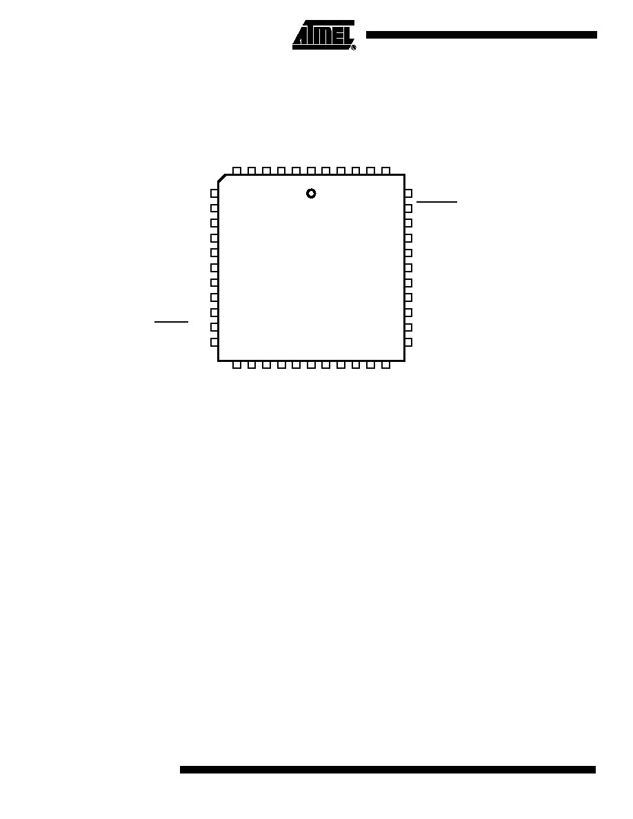
Pin Configuration
44-lead PLCC
7
8
9
10
11
12
13
14
15
16
17
39
38
37
36
35
34
33
32
31
30
29
6
5
4
3
2
1
44
43
42
41
40
18
19
20
21
22
23
24
25
26
27
28
NC
GND
PAGESEL0
NC
NC
NC
NC
NC
NC
NC
nCASC/A2
NC
NC
NC
NC
DATA
PAGE_EN
NC
NC
NC
VCC
NC
NC
DCLK
NC
NC
NC
NC
NC
NC
NC
RESET/OE
nCS
NC
SER_EN
NC
NC
READY
NC
PAGESEL1
NC
NC
NC
NC

3
AT17F32A
3489A≠CNFG≠6/04
Block Diagram
Device Description
The control signals for the configuration memory device (nCS, RESET/OE and DCLK)
interface directly with the FPGA device control signals. All FPGA devices can control the
entire configuration process and retrieve data from the configuration device without
requiring an external intelligent controller.
The RESET/OE and nCS pins control the tri-state buffer on the DATA output pin and
enable the address counter. When RESET/OE is driven Low, the configuration device
resets its address counter and tri-states its DATA pin. The nCS pin also controls the out-
put of the AT17FxxA Series Configurator. If nCS is held High after the RESET/OE reset
pulse, the counter is disabled and the DATA output pin is tri-stated. When OE is subse-
quently driven High, the counter and the DATA output pin are enabled. When
RESET/OE is driven Low again, the address counter is reset and the DATA output pin is
tri-stated, regardless of the state of nCS.
When the configurator has driven out all of its data and nCASC is driven Low, the device
tri-states the DATA pin to avoid contention with other configurators. Upon power-up, the
address counter is automatically reset.
Config. Page
Select
Power-on
Reset
Flash
Memory
Clock/Oscillator
Logic
2-wire Serial Programming
Serial Download Logic
Control Logic
DCLK
nCASC(A2)
DATA
nCS
RESET/OE
SER_EN
CE/WE/OE
Data
Address
READY
PAGE_EN
PAGESEL0
PAGESEL1
Reset

4
AT17F32A
3489A≠CNFG≠6/04
DATA
(1)
Three-state DATA output for FPGA configuration. Open-collector bi-directional pin for
configuration programming.
DCLK
(1)
Three-state clock. Functions as an input when the Configurator is in programming mode
(i.e. SER_EN is Low) and as an output during FPGA configuration.
PAGE_EN
(2)
Input used to enable page download mode. When PAGE_EN is high the configuration
download address space is partitioned into 4 equal pages. This gives users the ability to
easily store and retrieve multiple configuration bitstreams from a single configuration
device. This input works in conjunction with the PAGESEL inputs. PAGE_EN must be
remain low if paging is not desired. When SER_EN is Low (ISP mode) this pin has no
effect.
Notes:
1. This pin has an internal 20 K
pull-up resistor.
2. This pin has an internal 30 K
pull-down resistor.
Pin Description
Name
I/O
AT17F32A
44
PLCC
DATA
I/O
2
DCLK
I/O
8
PAGE_EN
I
1
PAGESEL0
I
20
PAGESEL1
I
33
RESET/OE
I
16
nCS
I
17
GND
≠
19
nCASC
O
28
A2
I
READY
O
35
SER_EN
I
38
V
CC
≠
41

5
AT17F32A
3489A≠CNFG≠6/04
PAGESEL[1:0]
(2)
Page select inputs. Used to determine which of the 4 memory pages are targeted during
a serial configuration download. The address space for each of the pages is shown in
Table 2. When SER_EN is Low (ISP mode) these pins have no effect.
RESET/OE
(1)
Output Enable (active High) and RESET (active Low) when SER_EN is High. A Low
level on RESET/OE resets both the address and bit counters. A High level (with nCS
Low) enables the data output driver.
nCS
(1)
Chip Enable input (active Low). A Low level (with OE High) allows DCLK to increment
the address counter and enables the data output driver. A High level on nCS disables
both the address and bit counters and forces the device into a low-power standby mode.
Note that this pin will not enable/disable the device in the 2-wire Serial Programming
mode (SER_EN Low).
GND
Ground pin. A 0.2 µF decoupling capacitor between V
CC
and GND is recommended.
nCASC
Cascade Select Output (when SER_EN is High). This output goes Low when the inter-
nal address counter has reached its maximum value. If the PAGE_EN input is set High,
the maximum value is the highest address in the selected partition. The PAGESEL[1:0]
inputs are used to make the 4 partition selections. If the PAGE_EN input is set Low, the
device is not partitioned and the address maximum value is the highest address in the
device, see Table 2 on page 5. In a daisy chain of AT17FxxA Series devices, the
nCASC pin of one device must be connected to the nCS input of the next device in the
chain. It will stay Low as long as nCS is Low and OE is High. It will then follow nCS until
OE goes Low; thereafter, nCASC will stay High until the entire EEPROM is read again.
A2
(1)
Device selection input, (when SER_EN Low). The input is used to enable (or chip
select) the device during programming (i.e., when SER_EN is Low). Refer to the
AT17FxxA Programming Specification available on the Atmel web site for additional
details.
READY
Open collector reset state indicator. Driven Low during power-up reset, released when
power-up is complete. (recommended 4.7 k
pull-up on this pin if used).
SER_EN
(1)
The serial enable input must remain High during FPGA configuration operations. Bring-
ing SER_EN Low enables the 2-Wire Serial Programming Mode. For non-ISP
applications, SER_EN should be tied to V
CC
.
V
CC
+3.3V (±10%).
Notes:
1. This pin has an internal 20 K
pull-up resistor.
2. This pin has an internal 30 K
pull-down resistor.
Table 2. Address Space
Paging Decodes
AT17F32A (32 Mbits)
PAGESEL = 00, PAGE_EN = 1
000000 ≠ 07FFFFh
PAGESEL = 01, PAGE_EN = 1
080000 ≠ 0FFFFFh
PAGESEL = 10, PAGE_EN = 1
100000 ≠ 17FFFFh
PAGESEL = 11, PAGE_EN = 1
180000 ≠ 1FFFFFh
PAGESEL = XX, PAGE_EN = 0
000000 ≠ 1FFFFFh