1
Features
∑
Write Protect Pin for Hardware Data Protection
≠ Utilizes Different Array Protection Compared to the AT24C02/04/08
∑
Low Voltage and Standard Voltage Operation
≠ 5.0 (V
CC
= 4.5V to 5.5V)
≠ 2.7 (V
CC
= 2.7V to 5.5V)
≠ 2.5 (V
CC
= 2.5V to 5.5V)
≠ 1.8 (V
CC
= 1.8V to 5.5V)
∑
Internally Organized 256 x 8 (2K), 512 x 8 (4K) or 1024 x 8 (8K)
∑
2-Wire Serial Interface
∑
Schmitt Trigger, Filtered Inputs for Noise Supperssion
∑
Bidirectional Data Transfer Protocol
∑
100 kHz (1.8V, 2.5V, 2.7V) and 400 kHz (5V) Compatibility
∑
8-Byte Page (2K), 16-Byte Page (4K, 8K) Write Modes
∑
Partial Page Writes Are Allowed
∑
Self-Timed Write Cycle (10 ms max)
∑
High Reliability
≠ Endurance: 1 Million Write Cycles
≠ Data Retention: 100 Years
≠ ESD Protection: >3000V
∑
Automotive Grade and Extended Temperature Devices Available
∑
8-Pin and 14-Pin JEDEC SOIC, 8-Pin PDIP, and 8-Pin TSSOP Packages
Description
The AT24C02A/04A/08A provides 2048/4096/8192 bits of serial electrically erasable
and programmable read only memory (EEPROM) organized as 256/512/1024 words
of 8 bits each. The device is optimized for use in many industrial and commercial
applications where low power and low voltage operation are essential. The
AT24C02A/04A/08A is available in space saving 8-pin PDIP, 8-pin, 14-pin SOIC, and
8-pin TSSOP packages and is accessed via a 2-wire serial interface. In addition, the
entire family is available in 5.0V (4.5V to 5.5V), 2.7V (2.7V to 5.5V), 2.5V (2.5V to
5.5V) and 1.8V (1.8V to 5.5V) versions.
2-Wire Serial
EEPROM
2K (256 x 8)
4K (512 x 8)
8K (1024 x 8)
AT24C02A
AT24C04A
AT24C08A
Rev. 0976B≠07/98
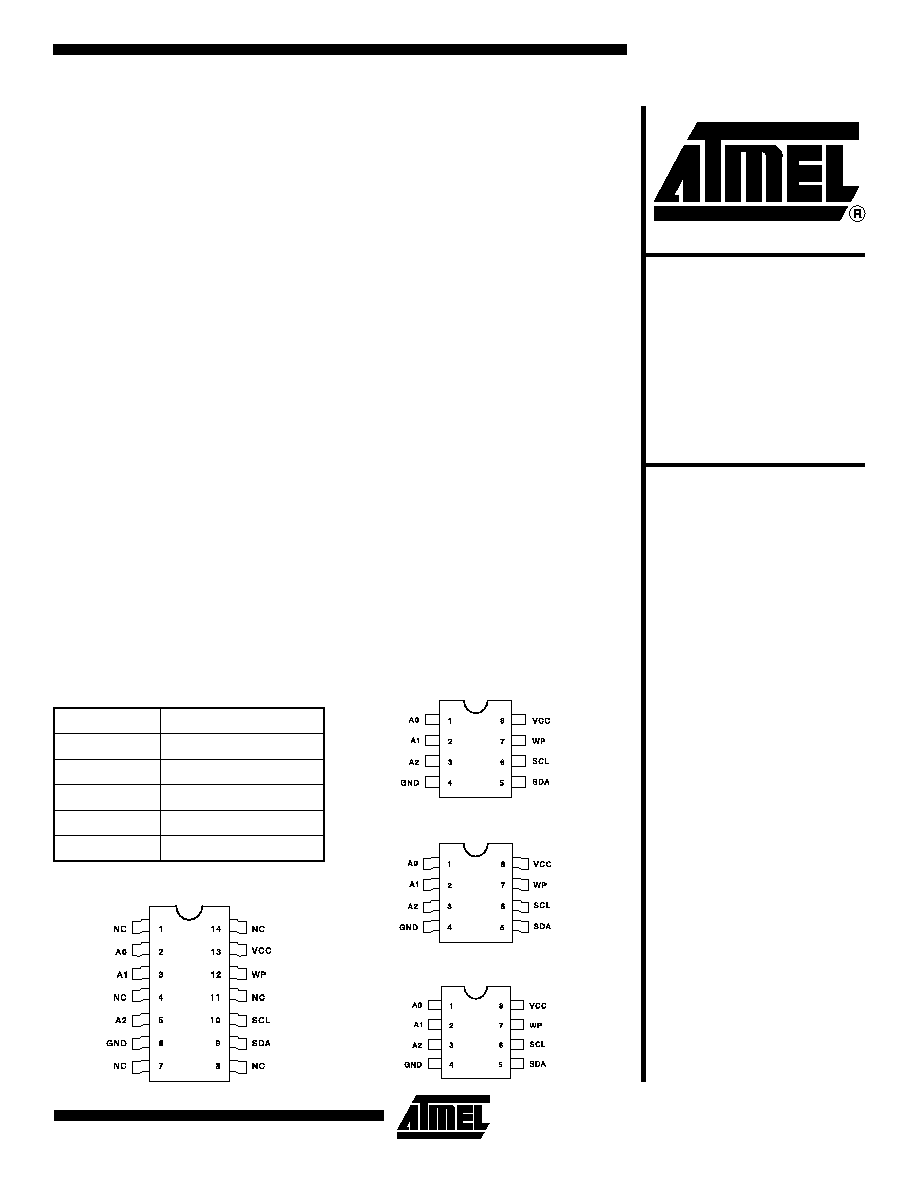
Pin Configurations
Pin Name
Function
A
0
to A
2
Address Inputs
SDA
Serial Data
SCL
Serial Clock Input
WP
Write Protect
NC
No Connect
14-Pin SOIC
8-Pin PDIP
8-Pin SOIC
AT24C02A/04A/
08A
8-Pin TSSOP
AT24C02A/04A/08A
2
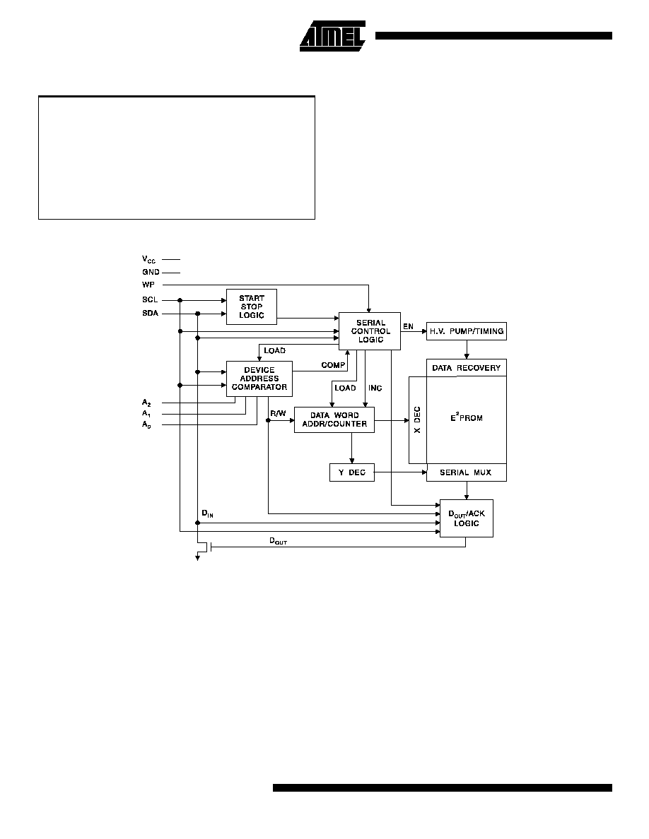
Block Diagram
Pin Description
SERIAL CLOCK (SCL): The SCL input is used to positive
edge clock data into each EEPROM device and negative
edge clock data out of each device.
SERIAL DATA (SDA): The SDA pin is bidirectional for
serial data transfer. This pin is open-drain driven and may
be wire-ORed with any number of other open-drain or open
collector devices.
DEVICE/PAGE ADDRESSES (A2, A1, A0): The A2, A1
and A0 pins are device address inputs that are hard wired
for the AT24C02A. As many as eight 2K devices may be
addressed on a single bus system (device addressing is
discussed in detail under the Device Addressing section).
The AT24C04A uses the A2 and A1 inputs for hard wire
a dd re s s i n g a n d a t ot a l o f fo u r 4K d e v i c e s m a y b e
addressed on a single bus system. The A0 pin is a no con-
nect.
The AT24C08A only uses the A2 input for hardwire
a d d r e s s i n g a n d a t o t a l o f t w o 8 K d e v i c e s m a y b e
addressed on a single bus system. The A0 and A1 pins are
no connects.
WRITE PROTECT (WP): The AT24C02A/04A/08A has a
Write Protect pin that provides hardware data protection.
The Write Protect pin allows normal read/write operations
when connected to ground (GND). When the Write Protect
Absolute Maximum Ratings*
Operating Temperature .................................. -55
∞
C to +125
∞
C
*NOTICE:
Stresses beyond those listed under "Absolute
Maximum Ratings" may cause permanent dam-
age to the device. This is a stress rating only and
functional operation of the device at these or any
other conditions beyond those indicated in the
operational sections of this specification is not
implied. Exposure to absolute maximum rating
conditions for extended periods may affect device
reliability.
Storage Temperature ..................................... -65
∞
C to +150
∞
C
Voltage on Any Pin
with Respect to Ground .....................................-1.0V to +7.0V
Maximum Operating Voltage........................................... 6.25V
DC Output Current........................................................ 5.0 mA
AT24C02A/04A/08A
3
pin is connected to V
CC
, the write protection feature is
enabled and operates as shown in the following table.
Memory Organization
AT24C02A, 2K SERIAL EEPROM: Internally organized
with 256 pages of 1-byte each, the 2K requires an 8 bit
data word address for random word addressing.
AT24C04A, 4K SERIAL EEPROM: The 4K is internally
organized with 256 pages of 2-bytes each. Random word
addressing requires a 9 bit data word address.
AT24C08A, 8K SERIAL EEPROM: The 8K is internally
organized with 4 blocks of 256 pages of 4-bytes each.
Random word addressing requires a 10 bit data word
address.
Note:
1. This parameter is characterized and is not 100% tested.
Note:
1. V
IL
min and V
IH
max are reference only and are not tested.
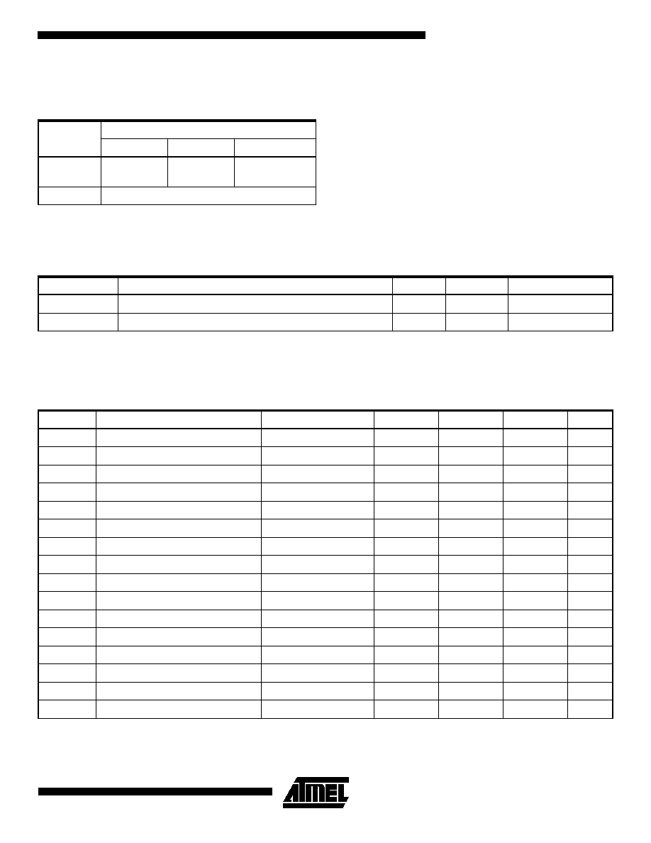
WP Pin
Status
Part of the Array Protected
24C02A
24C04A
24C08A
At V
CC
Upper Half
(1K) Array
Upper Half
(2K) Array
Full (8K)
Array
At GND
Normal Read/Write Operations
Pin Capacitance
Applicable over recommended operating range from T
A
= 25
∞
C, f = 1.0 MHz, V
CC
= +1.8V.
Symbol
Test Condition
Max
Units
Conditions
C
I/O
Input/Output Capacitance (SDA)
8
pF
V
I/O
= 0V
C
IN
Input Capacitance (A
0
, A
1
, A
2
, SCL)
6
pF
V
IN
= 0V
DC Characteristics
Applicable over recommended operating range from: T
AI
= -40
∞
C to +85
∞
C, V
CC
= +1.8V to +5.5V, T
AC
= 0
∞
C to +70
∞
C,
V
CC
= +1.8V to +5.5V (unless otherwise noted).
Symbol
Parameter
Test Condition
Min
Typ
Max
Units
V
CC1
Supply Voltage
1.8
5.5
V
V
CC2
Supply Voltage
2.5
5.5
V
V
CC3
Supply Voltage
2.7
5.5
V
V
CC4
Supply Voltage
4.5
5.5
V
I
CC
Supply Current V
CC
= 5.0V
READ at 100 kHz
0.4
1.0
mA
I
CC
Supply Current V
CC
= 5.0V
WRITE at 100 kHz
2.0
3.0
mA
I
SB1
Standby Current V
CC
= 1.8V
V
IN
= V
CC
or V
SS
0.6
3.0
µ
A
I
SB2
Standby Current V
CC
= 2.5V
V
IN
= V
CC
or V
SS
1.4
4.0
µ
A
I
SB3
Standby Current V
CC
= 2.7V
V
IN
= V
CC
or V
SS
1.6
4.0
µ
A
I
SB4
Standby Current V
CC
= 5.0V
V
IN
= V
CC
or V
SS
8.0
18.0
µ
A
I
LI
Input Leakage Current
V
IN
= V
CC
or V
SS
0.10
3.0
µ
A
I
LO
Output Leakage Current
V
OUT
= V
CC
or V
SS
0.05
3.0
µ
A
V
IL
Input Low Level
(1)
-0.6
V
CC
x 0.3
V
V
IH
Input High Level
(1)
V
CC
x 0.7
V
CC
+ 0.5
V
V
OL2
Output Low Level V
CC
= 3.0V
I
OL
= 2.1 mA
0.4
V
V
OL1
Output Low Level V
CC
= 1.8V
I
OL
= 0.15 mA
0.2
V
AT24C02A/04A/08A
4
Note:
1. This parameter is characterized and is not 100% tested.
Device Operation
CLOCK and DATA TRANSITIONS: The SDA pin is nor-
mally pulled high with an external device. Data on the SDA
pin may change only during SCL low time periods (refer to
Data Validity timing diagram). Data changes during SCL
high periods will indicate a start or stop condition as
defined below.
START CONDITION: A high-to-low transition of SDA with
SCL high is a start condition which must precede any other
command (refer to Start and Stop Definition timing dia-
gram).
STOP CONDITION: A low-to-high transition of SDA with
SCL high is a stop condition. After a read sequence, the
stop command will place the EEPROM in a standby power
mode (refer to Start and Stop Definition timing diagram).
ACKNOWLEDGE: All addresses and data words are seri-
ally transmitted to and from the EEPROM in 8 bit words
.
The
EEPROM sends a zero to acknowledge that it has
received each word. This happens during the ninth clock
cycle.
STANDBY MODE: The AT24C02A/04A/08A features a low
power standby mode which is enabled: (a) upon power-up
and (b) after the receipt of the STOP bit and the completion
of any internal operations.
MEMORY RESET: After an interruption in protocol, power
loss or system reset, any 2-wire part can be reset by follow-
ing these steps:(a) Clock up to 9 cycles, (b) look for SDA
high in each cycle while SCL is high and then (c) create a
start condition as SDA is high.
AC Characteristics
Applicable over recommended operating range from T
A
= -40
∞
C to +85
∞
C, V
CC
= +1.8V to +5.5V, CL = 1 TTL Gate and
100 pF (unless otherwise noted).
Symbol
Parameter
2.7-, 2.5-, 1.8-volt
5.0-volt
Units
Min
Max
Min
Max
f
SCL
Clock Frequency, SCL
100
400
kHz
t
LOW
Clock Pulse Width Low
4.7
1.2
µ
s
t
HIGH
Clock Pulse Width High
4.0
0.6
µ
s
t
I
Noise Suppression Time
(1)
100
50
ns
t
AA
Clock Low to Data Out Valid
0.1
4.5
0.1
0.9
µ
s
t
BUF
Time the bus must be free before
a new transmission can start
(1)
4.7
1.2
µ
s
t
HD.STA
Start Hold Time
4.0
0.6
µ
s
t
SU.STA
Start Set-up Time
4.7
0.6
µ
s
t
HD.DAT
Data In Hold Time
0
0
µ
s
t
SU.DAT
Data In Set-up Time
200
100
ns
t
R
Inputs Rise Time
(1)
1.0
0.3
µ
s
t
F
Inputs Fall Time
(1)
300
300
ns
t
SU.STO
Stop Set-up Time
4.7
0.6
µ
s
t
DH
Data Out Hold Time
100
50
ns
t
WR
Write Cycle Time
10
10
ms
Endurance
(1)
5.0V, 25
∞
C, Page Mode
1M
1M
Write
Cycles
AT24C02A/04A/08A
5
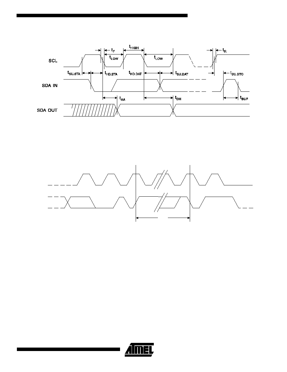
Bus Timing (SCL: Serial Clock, SDA: Serial Data I/O)
Write Cycle Timing (SCL: Serial Clock, SDA: Serial Data I/O)
Note:
1.
The write cycle time t
WR
is the time from a valid stop condition of a write sequence to the end of the interval
clear/write cycle.
SCL
SDA
8th BIT
WORD n
ACK
STOP
CONDITION
START
CONDITION
t
WR
(1)