1
Features
∑
Serial Peripheral Interface (SPI) Compatible
∑
Supports SPI Modes 0 (0,0) and 3 (1,1)
∑
Low-voltage and Standard-voltage Operation
≠ 5.0 (V
CC
= 4.5V to 5.5V)
≠ 2.7 (V
CC
= 2.7V to 5.5V)
≠ 1.8 (V
CC
= 1.8V to 3.6V)
∑
3.0 MHz Clock Rate (5V)
∑
32-byte Page Mode
∑
Block Write Protection
≠ Protect 1/4, 1/2, or Entire Array
∑
Write Protect (WP) Pin and Write Disable Instructions for
both Hardware and Software Data Protection
∑
Self-timed Write Cycle (5 ms Typical)
∑
High-reliability
≠ Endurance: One Million Write Cycles
≠ Data Retention: 100 Years
∑
Automotive Grade and Extended Temperature Devices Available
∑
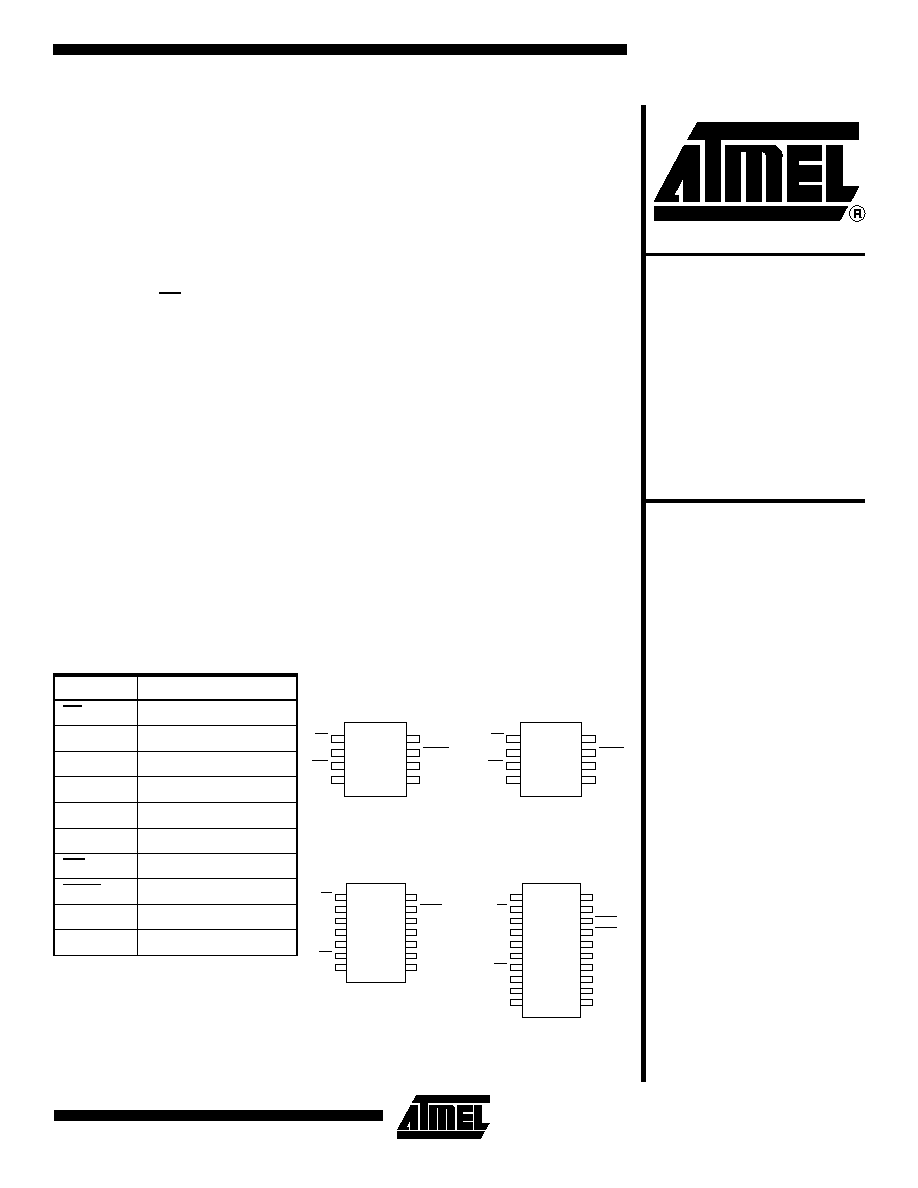
8-pin PDIP, 8-lead JEDEC SOIC, and 14-lead and 20-lead TSSOP Packages
Description
The AT25080/160/320/640 provides 8192/16384/32768/65536 bits of serial electri-
cally-erasable programmable read only memory (EEPROM) organized as
1024/2048/4096/8192 words of 8 bits each. The device is optimized for use in many
industrial and commercial applications where low-power and low-voltage operation
are essential. The AT25080/160/320/640 is available in space saving 8-pin PDIP, 8-
lead JEDEC SOIC, and 14-lead and 20-lead TSSOP packages.
SPI Serial
EEPROMs
8K (1024 x 8)
16K (2048 x 8)
32K (4096 x 8)
64K (8192 x 8)
AT25080
AT25160
AT25320
AT25640
Rev. 0675F≠08/01
Pin Configuration
Pin Name
Function
CS
Chip Select
SCK
Serial Data Clock
SI
Serial Data Input
SO
Serial Data Output
GND
Ground
VCC
Power Supply
WP
Write Protect
HOLD
Suspends Serial Input
NC
No Connect
DC
Don't Connect
8-pin PDIP
1
2
3
4
8
7
6
5
CS
SO
WP
GND
VCC
HOLD
SCK
SI
8-lead SOIC
1
2
3
4
8
7
6
5
CS
SO
WP
GND
VCC
HOLD
SCK
SI
14-lead TSSOP
1
2
3
4
5
6
7
14
13
12
11
10
9
8
CS
SO
NC
NC
NC
WP
GND
VCC
HOLD
NC
NC
NC
SCK
SI
20-lead TSSOP*
1
2
3
4
5
6
7
8
9
10
20
19
18
17
16
15
14
13
12
11
NC
CS
SO
SO
NC
NC
WP
GND
DC
NC
NC
VCC
HOLD
HOLD
NC
NC
SCK
SI
DC
NC
Note:
*Pins 3, 4 and 17, 18 are internally connected
for 14-lead TSSOP socket compatibility.
(continued)
2
AT25080/160/320/640
0675F≠08/01
The AT25080/160/320/640 is enabled through the Chip Select pin (CS) and accessed via a 3-
wire interface consisting of Serial Data Input (SI), Serial Data Output (SO), and Serial Clock
(SCK). All programming cycles are completely self-timed, and no separate ERASE cycle is
required before WRITE.
BLOCK WRITE protection is enabled by programming the status register with one of four
blocks of write protection. Separate program enable and program disable instructions are pro-
vided for additional data protection. Hardware data protection is provided via the WP pin to
protect against inadvertent write attempts to the status register. The HOLD pin may be used to
suspend any serial communication without resetting the serial sequence.
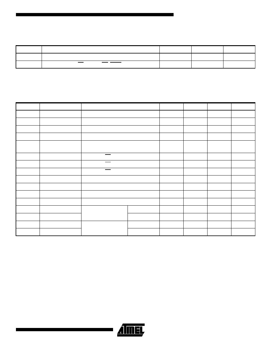
Block Diagram
Absolute Maximum Ratings*
Operating Temperature.................................. -55
∞C to +125∞C
*NOTICE:
Stresses beyond those listed under "Absolute
Maximum Ratings" may cause permanent dam-
age to the device. This is a stress rating only and
functional operation of the device at these or any
other conditions beyond those indicated in the
operational sections of this specification is not
implied. Exposure to absolute maximum rating
conditions for extended periods may affect device
reliability.
Storage Temperature ..................................... -65
∞C to +150∞C
Voltage on Any Pin
with Respect to Ground .....................................-1.0V to +7.0V
Maximum Operating Voltage .......................................... 6.25V
DC Output Current........................................................ 5.0 mA
3
AT25080/160/320/640
0675F≠08/01
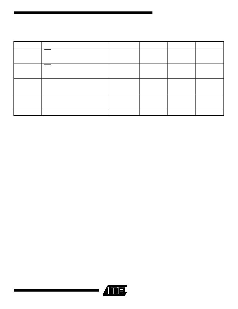
Pin Capacitance
(1)
Note:
1. This parameter is characterized and is not 100% tested.
DC Characteristics
(1)
Note:
1. V
IL
min and V
IH
max are reference only and are not tested.
Applicable over recommended operating range from T
A
= 25
∞C, f = 1.0 MHz, V
CC
= +5.0V (unless otherwise noted).
Symbol
Test Conditions
Max
Units
Conditions
C
OUT
Output Capacitance (SO)
8
pF
V
OUT
= 0V
C
IN
Input Capacitance(CS, SCK, SI, WP, HOLD)
6
pF
V
IN
= 0V
Applicable over recommended operating range from: T
AI
= -40
∞C to +85∞C, V
CC
= +1.8V to +5.5V, T
AC
= 0
∞C to +70∞C,
V
CC
= +1.8V to +5.5V (unless otherwise noted).
Symbol Parameter
Test
Condition
Min
Typ
Max
Units
V
CC1
Supply
Voltage
1.8
3.6
V
V
CC2
Supply Voltage
2.7
5.5
V
V
CC3
Supply
Voltage
4.5
5.5
V
I
CC1
Supply
Current
V
CC
= 5.0V at 1 MHz, SO = Open, Read
3.0
mA
I
CC2
Supply
Current
V
CC
= 5.0V at 2 MHz, SO = Open,
Read, Write
5.0
mA
I
SB1
Standby
Current
V
CC
= 1.8V, CS = V
CC
0.1
1.0
µA
I
SB2
Standby
Current
V
CC
= 2.7V, CS = V
CC
0.2
2.0
µA
I
SB3
Standby Current
V
CC
= 5.0V, CS = V
CC
2.0
5.0
µA
I
IL
Input
Leakage
V
IN
= 0V to V
CC
-3.0
µA
I
OL
Output Leakage
V
IN
= 0V to V
CC
, T
AC
= 0∞C to 70∞C
-3.0
3.0
µA
V
IL
(1)
Input Low-voltage
-0.6
V
CC
x 0.3
V
V
IH
(1)
Input High-voltage
V
CC
x 0.7
V
CC
+ 0.5
V
V
OL1
Output
Low-voltage
4.5V
V
CC
5.5V
I
OL
= 3.0 mA
0.4
V
V
OH1
Output High-voltage
I
OH
= -1.6 mA
V
CC
- 0.8
V
V
OL2
Output Low-voltage
1.8V
V
CC
3.6V
I
OL
= 0.15 mA
0.2
V
V
OH2
Output High-voltage
I
OH
= -100 µA
V
CC
- 0.2
V
4
AT25080/160/320/640
0675F≠08/01
AC Characteristics
Applicable over recommended operating range from T
A
= -40
∞C to +85∞C, V
CC
= As Specified,
CL = 1 TTL Gate and 100 pF (unless otherwise noted).
Symbol
Parameter
Voltage
Min
Max
Units
f
SCK
SCK Clock Frequency
4.5 - 5.5
2.7 - 5.5
1.8 - 3.6
0
0
0
3.0
2.1
0.5
MHz
t
RI
Input Rise Time
4.5 - 5.5
2.7 - 5.5
1.8 - 3.6
2
2
2
µs
t
FI
Input Fall Time
4.5 - 5.5
2.7 - 5.5
1.8 - 3.6
2
2
2
µs
t
WH
SCK High Time
4.5 - 5.5
2.7 - 5.5
1.8 - 3.6
133
200
800
ns
t
WL
SCK Low Time
4.5 - 5.5
2.7 - 5.5
1.8 - 3.6
133
200
800
ns
t
CS
CS High Time
4.5 - 5.5
2.7 - 5.5
1.8 - 3.6
250
250
1000
ns
t
CSS
CS Setup Time
4.5 - 5.5
2.7 - 5.5
1.8 - 3.6
250
250
1000
ns
t
CSH
CS Hold Time
4.5 - 5.5
2.7 - 5.5
1.8 - 3.6
250
250
1000
ns
t
SU
Data In Setup Time
4.5 - 5.5
2.7 - 5.5
1.8 - 3.6
50
50
100
ns
t
H
Data In Hold Time
4.5 - 5.5
2.7 - 5.5
1.8 - 3.6
50
50
100
ns
t
HD
Hold Setup Time
4.5 - 5.5
2.7 - 5.5
1.8 - 3.6
100
100
400
t
CD
Hold Hold Time
4.5 - 5.5
2.7 - 5.5
1.8 - 3.6
200
200
400
ns
t
V
Output Valid
4.5 - 5.5
2.7 - 5.5
1.8 - 3.6
0
0
0
133
200
800
ns
t
HO
Output Hold Time
4.5 - 5.5
2.7 - 5.5
1.8 - 3.6
0
0
0
ns
5
AT25080/160/320/640
0675F≠08/01
Note:
1. This parameter is characterized and is not 100% tested.
t
LZ
Hold to Output Low Z
4.5 - 5.5
2.7 - 5.5
1.8 - 3.6
0
0
0
100
100
100
ns
t
HZ
Hold to Output High Z
4.5 - 5.5
2.7 - 5.5
1.8 - 3.6
100
100
100
ns
t
DIS
Output Disable Time
4.5 - 5.5
2.7 - 5.5
1.8 - 3.6
250
250
1000
ns
t
WC
Write Cycle Time
4.5 - 5.5
2.7 - 5.5
1.8 - 3.6
5
10
20
ms
Endurance
(1)
5.0V, 25∞C, Page Mode
1M
Write Cycles
AC Characteristics (Continued)
Applicable over recommended operating range from T
A
= -40
∞C to +85∞C, V
CC
= As Specified,
CL = 1 TTL Gate and 100 pF (unless otherwise noted).
Symbol
Parameter
Voltage
Min
Max
Units