1
Features
∑
Fast Interleave Cycle Time - 35 ns
∑
Continuous Memory Interleaving
≠ Unlimited Linear Access Data Output
∑
Dual Voltage Range Operation
≠ Low Voltage Power Supply Range, 3.0V to 3.6V
or Standard 5V
±
±
±
±
10% Supply Range
∑
Low Power CMOS Operation
≠ 108 mW max. Active at 25 MHz for V
CC
= 3.6V
≠ 14.4 mW max. Standby for V
CC
= 3.6V
∑
JEDEC Standard Surface Mount Packages
≠ 44-Lead PLCC
≠ 40-Lead VSOP (10 x 14mm)
∑
High Reliability CMOS Technology
≠ 2,000V ESD Protection
≠ 200 mA Latchup Immunity
∑
Rapid
TM
Programming Algorithm - 50
µ
µ
µ
µ
s/word (typical)
∑
CMOS and TTL Compatible Inputs and Outputs
≠ JEDEC Standard for LVTTL
∑
Integrated Product Identification Code
∑
Commercial and Industrial Temperature Ranges
Description
The AT27LV1026 is a high performance 16-bit interleaved low-voltage 1,048,576-bit
one-time programmable read only memory (OTP EPROM) organized as 2 x 32K x 16
bits. It requires only one supply in the range of 3.0V to 3.6V in normal read mode
operation.
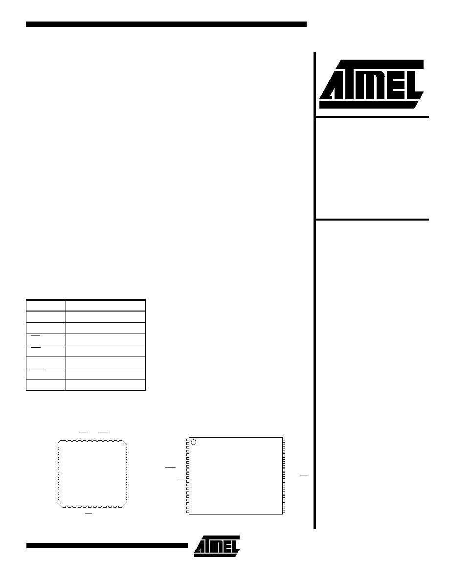
Pin Configurations
Note:
Both GND pins must be
connected.
Pin Name
Function
A0 - A15
Addresses
O0 - O15
Outputs
CS
Chip Select
RD
Read Strobe
ALE
Address Latch Enable
PGM
Program Strobe
NC
No Connect
Rev. 0956D≠02/98
1-Megabit
(2 x 32K x 16)
16-Bit Interleaved
Low-Voltage OTP
EPROM
AT27LV1026
Preliminary
PLCC Top View
VSOP Top View
Type 1
7
8
9
10
11
12
13
14
15
16
17
6
5
4
3
1
44
43
42
41
40
39
38
37
36
35
34
33
32
31
30
29
18
19
20
21
22
23
24
25
26
27
28
O13
O14
O15
CS
VPP
GND
VCC
PGM
ALE
A15
A14
O3
O2
O1
O0
RD
GND
A0
A1
A2
A3
A4
A13
A12
A11
A10
A9
A8
A7
A6
A5
O12
O11
O10
O9
O8
O7
O6
O5
O4
GND
NC
GND
NC
2
A11
A12
A14
A13
ALE
PGM
A15
O14
O12
O13
CS
O15
VPP
VCC
1
2
4
3
6
5
10
9
7
8
14
13
11
12
O2
O1
O3
O4
A0
A1
RD
O0
A3
A2
A5
A4
A6
A7
33
32
30
31
28
27
29
36
34
35
38
37
39
40
25
26
O6
O5
15
16
O11
O10
O9
20
19
O7
GND
22
21
23
24
17
18
O8
A9
A10
A8
GND
AT27LV1026
2
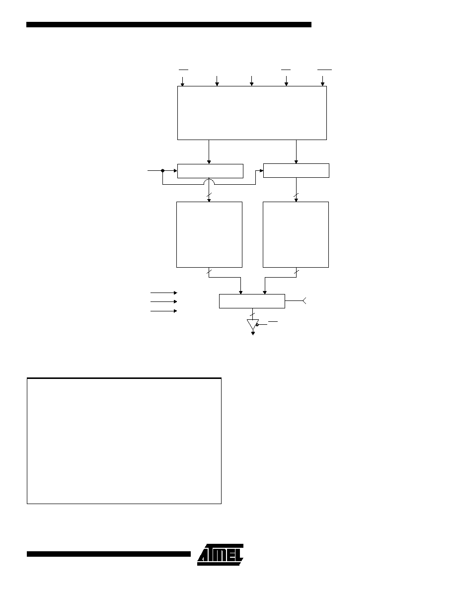
This device is internally architected as two 32K x 16 mem-
ory banks, odd and even. To begin a non-linear access
NLA cycle, (which typically equals a minimum of two linear
access LA cycles), ALE is asserted high and CS is
asserted low. The two internal 15-bit counters store the
address for the odd and even banks and increment alter-
nately during each subsequent linear access LA cycle. The
LA cycle will be terminated when CS is asserted high put-
ting the device in standby mode, or another NLA cycle
starts. The LA cycle can be resumed when CS is asserted
low and ALE stays low. The AT27LV1026 will continuously
output data within each LA cycle which is determined by
the read RD signal. Continuous interleave read operation is
possible as there is no physical limit to the linear access LA
output. When the last address in the array is reached the
counters will wrap around to the first address location and
continue.
For a NLA cycle where A0 = 0 (ALE asserted high, CS
asserted low), both even and odd counters will be loaded
with new address (A1 - A15). Outputs (O0 - O15) from the
even bank will be valid in t
ACCNLA
within the NLA cycle, the
outputs from the odd bank will become valid in t
ACCLA
within
the following LA cycle while the even counter increments
by one to ready the data out for the next LA cycle. The out-
puts will have even or odd data alternating and the
counters increment for the consecutive LA cycles until CS
is asserted high putting the device in standby mode, or a
new NLA cycle begins.
For a NLA cycle where A0 = 1 (ALE asserted high, CS
asserted low), the odd counter will be loaded with the new
address (A1 - A15) while the even counter gets loaded with
the new address+1. Outputs (O0 - O15) from odd bank of
memory will be valid in t
ACCNLA
within the NLA cycle, the
data output from the even bank of memory will become
valid in t
ACCLA
within the following LA cycle while the odd
counter increments by one to ready the data out for the
next LA cycle. The outputs will have data from the odd or
even memory bank alternately and the counters increment
for the following consecutive LA cycles until CS is asserted
high putting the device in standby mode, or a new NLA
cycle begins. When coming out of standby mode, the
device can either enter into a new NLA cycle or resume
where the previous LA operation left off and was termi-
nated by standby mode.
System Considerations
Switching under active conditions may produce transient
voltage excursions. Unless accommodated by the system
design, these transients may exceed data sheet limits,
resulting in device non-conformance. At a minimum, a 0.1
µ
F high frequency, low inherent inductance, ceramic
capacitor should be utilized for each device. This capacitor
should be connected between the V
CC
and Ground termi-
nals of the device, as close to the device as possible. Addi-
tionally, to stabilize the supply voltage level on printed cir-
cuit boards with large EPROM arrays, a 4.7
µ
F bulk elec-
trolytic capacitor should be utilized, again connected
between the V
CC
and Ground terminals. This capacitor
should be positioned as close as possible to the point
where the power supply is connected to the array.
Operating Table
If A0 = 0 at beginning of NLA cycle:
If A0 = 1 at beginning of NLA cycle:
and so on.
and so on.
Consecutive
Cycle
Counter
Outputs
Consecutive
Cycle
Counter
Outputs
Even
Odd
Even
Odd
NLA
Address
Address
from Even Bank
NLA
Address+1
Address
from Odd Bank
LA
+1
-
from Odd Bank
LA
-
+1
from Even Bank
LA
-
+1
from Even Bank
LA
+1
-
from Odd Bank
LA
+1
-
from Odd Bank
LA
-
+1
from Even Bank
LA
-
+1
from Even Bank
LA
+1
-
from Odd Bank
Standby
HiZ
Standby
HiZ
LA
+1
-
from Odd Band
LA
-
+1
from Even Bank
LA
-
+1
from Even Bank
LA
+1
-
from Odd Band
AT27LV1026
3
Block Diagram
32K x 16
Memory
Array
32K x 16
Memory
Array
MUX
Logic
15
16
16
15
16
A0
CS
Data Outputs
O -O
0
1 5
ALE
A0
RD
CS
Odd Counter
CLK_EVEN
CLK_ODD
Even Counter
Address
Input
A -A
1
1 5
PGM
V
CC
GND
V
PP
Absolute Maximum Ratings*
Temperature Under Bias ................................ -55
∞
C to +125
∞
C
*NOTICE:
Stresses beyond those listed under "Absolute
Maximum Ratings" may cause permanent dam-
age to the device. This is a stress rating only and
functional operation of the device at these or any
other conditions beyond those indicated in the
operational sections of this specification is not
implied. Exposure to absolute maximum rating
conditions for extended periods may affect device
reliability.
Note:
1.
Minimum voltage is -0.6V DC which may under-
shoot to -2.0V for pulses of less than 20 ns. Max-
imum output pin voltage is V
CC
+ 0.75V DC which
may overshoot to +7.0V for pulses of less than 20
ns.
Storage Temperature ..................................... -65
∞
C to +150
∞
C
Voltage on Any Pin with
Respect to Ground .........................................-2.0V to +7.0V
(1)
Voltage on A9 with
Respect to Ground .......................................-2.0V to +14.0V
(1)
V
PP
Supply Voltage with
Respect to Ground .......................................-2.0V to +14.0V
(1)
AT27LV1026
4
Operating Modes
Notes:
1. X can be V
IL
or V
IH
.
2. Non-Linear and Linear Access Cycles, and standby modes require, 3.0V
V
CC
3.6V, or 4.5V
V
CC
5.5V.
3. Refer to Programming Characteristics. Programming modes require V
CC
= 6.5V.
4. V
H
= 12.0
±
0.5V.
5. Two identifier words may be selected. All Ai inputs are held low (V
IL
), except A9 which is set to V
H
and A0 which is toggled
low (V
IL
) to select the Manufacturer's Identification word and high (V
IH
) to select the Device Code word.
DC and AC Operating Conditions for Read Operation
Mode/Pin
ALE
CS
RD
PGM
A
0
A
1
- A
15
V
PP
V
CC
Outputs
Non-Linear Access Cycle
(2)
V
IL
V
IL
V
IH
V
IL
/V
IH
Ai
X
V
CC
(2)
D
OUT
Linear Access Cycle
(2)
V
IL
V
IL
V
IH
X
(1)
X
X
V
CC
(2)
D
OUT
Standby
(2)
X
V
IH
X
V
IH
X
X
X
V
CC
(2)
High Z
Rapid Program
(3)
V
IH
V
IH
V
IL
V
IL
V
IL
/V
IH
Ai
V
PP
V
CC
(3)
D
IN
PGM Verify
(3)
V
IH
V
IL
V
IL
V
IH
V
IL
/V
IH
Ai
V
PP
V
CC
(3)
D
OUT
PGM Inhibit
(3)
X
V
IH
X
V
IH
X
X
V
PP
V
CC
(3)
High Z
Product Identification
(3)(5)
X
V
IL
X
V
IH
V
IL
/V
IH
A
9
= V
H
(4)
A
1
- A
15
= V
IL
V
CC
V
CC
(3)
Identification Code
AT27LV1026
-35
-45
-55
Operating
Temperature (Case)
Com.
0
∞
C - 70
∞
C
0
∞
C - 70
∞
C
0
∞
C - 70
∞
C
Ind.
-40
∞
C - 85
∞
C
-40
∞
C - 85
∞
C
-40
∞
C - 85
∞
C
V
CC
Power Supply
3.0V - 3.6V
3.0V - 3.6V
3.0V - 3.6V
5V
±
10%
5V
±
10%
5V
±
10%
AT27LV1026
5
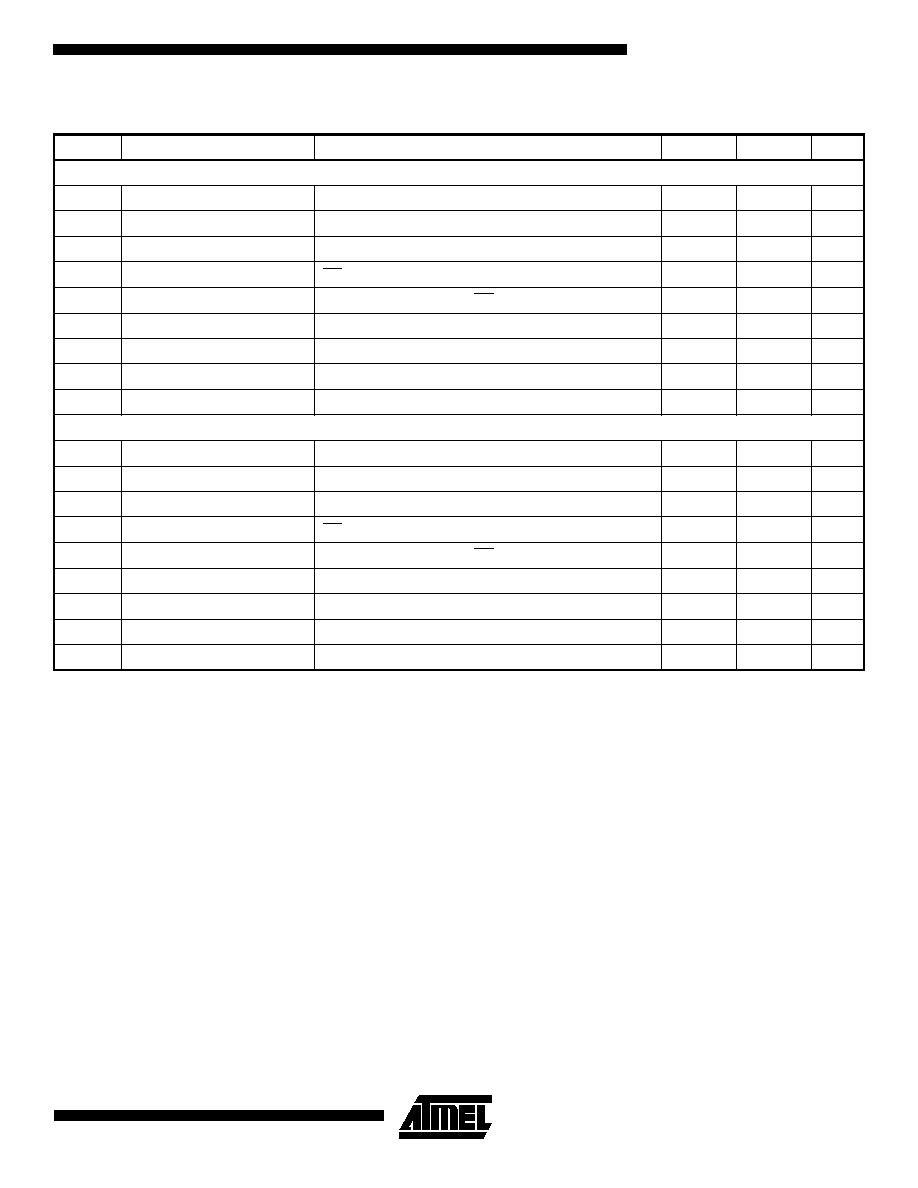
DC and Operating Characteristics for Read Operation
Notes:
1. V
CC
must be applied simultaneously with or before V
PP
, and removed simultaneously with or after V
PP
.
2. V
PP
may be connected directly to V
CC
, except during programming. The supply current would then be the sum of I
CC
and I
PP
.
Symbol
Parameter
Condition
Min
Max
Units
V
CC
= 3.0V to 3.6V
I
LI
Input Load Current
V
IN
= 0V to V
CC
±
1
µ
A
I
LO
Output Leakage Current
V
OUT
= 0V to V
CC
±
5
µ
A
I
PP1
(2)
V
PP
(1)
Read/Standby Current
V
PP
= V
CC
10
µ
A
I
SB
V
CC
(1)
Standby Current
CS = V
IH
4
mA
I
CC
V
CC
Active Current
f = 25 MHz, I
OUT
= 0 mA, CS = V
IL
30
mA
V
IL
Input Low Voltage
-0.6
0.8
V
V
IH
Input High Voltage
2.0
V
CC
+ 0.5
V
V
OL
Output Low Voltage
I
OL
= 2.0 mA
0.4
V
V
OH
Output High Voltage
I
OH
= -2.0
mA
2.4
V
V
CC
= 4.5V to 5.5V
I
LI
Input Load Current
V
IN
= 0V to V
CC
±
1
µ
A
I
LO
Output Leakage Current
V
OUT
= 0V to V
CC
±
5
µ
A
I
PP1
(2)
V
PP
(1)
Read/Standby Current
V
PP
= V
CC
10
µ
A
I
SB
V
CC
(1)
Standby Current
CS = V
IH
6
mA
I
CC
V
CC
Active Current
f = 25 MHz, I
OUT
= 0 mA, CS = V
IL
50
mA
V
IL
Input Low Voltage
-0.6
0.8
V
V
IH
Input High Voltage
2.0
V
CC
+ 0.5
V
V
OL
Output Low Voltage
I
OL
= 2.1 mA
0.4
V
V
OH
Output High Voltage
I
OH
= -400
µ
A
2.4
V