Rev. 4134A≠8051≠05/02
1
Features
∑
80C51-compatible CPU Core High-speed Architecture
∑
16 MHz at 3.3V
∑
X2 Speed Improvement Capability (6 Clocks/Machine Cycle)
∑
256 Bytes RAM
∑
256 Bytes XRAM
∑
12 Kbytes ROM/OTP Program Memory
∑
Two 16-bit Timer/Counters T0, T1
∑
5 Channels Programmable Counter Array with High-speed Output, Compare/Capture,
Pulse Width Modulation and Watchdog Timer Capabilities
∑
2 MHz SPI Serial Interface
∑
Interrupt Structure with:
≠ 5 Interrupt Sources
≠ 4 Interrupt Priority Levels
∑
Power Supply: 3 - 5V
±
10%
∑
Temperature Range: Industrial (-40
o
C to 85
o
C), Automotive (-40
o
C to 125
o
C)
∑
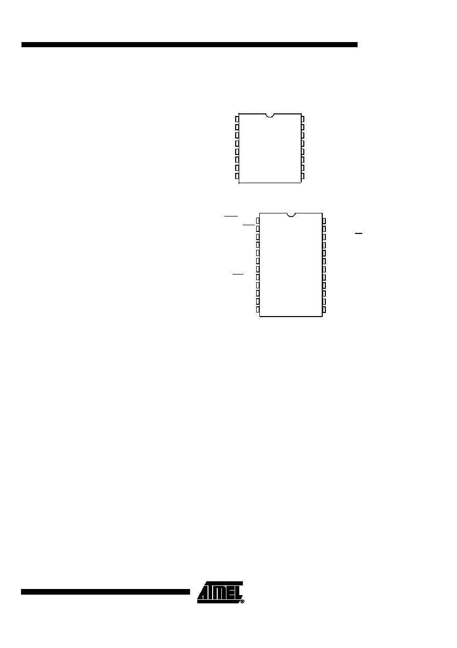
Package: SSOP16, SSOP24
Description
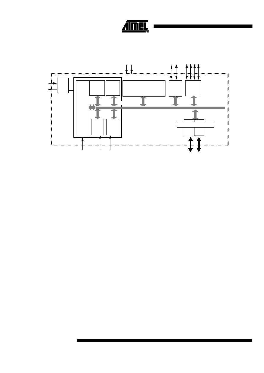
The AT8xC5103 is a high-performance ROM/OTP version of the 80C51 8-bit Micro-
controller in 16 and 24-pin packages.
The AT8xC5103 contains a standard C51 CPU core with 12 Kbytes ROM/OTP pro-
gram memory, 256 bytes of internal RAM, 256 bytes of extended internal RAM, a 5-
sources 4-level interrupt system, two timer/counters and a SPI serial bus controller.
The AT8xC5103 is also dedicated for analog interfacing applications. For this, it has a
five channels Programmable Counter Array.
In addition, the AT8xC5103 implements the X2 speed improvement mechanism. The
X2 feature allows to keep the same CPU power at a divided by two oscillator
frequency.
The fully static design of the AT8xC5103 allows to reduce system power consumption
by bringing the clock frequency down to any value, even DC, without loss of data.
Low-pin Count
8-bit
Microcontroller
AT87C5103
AT83C5103
Preliminary
4
AT8xC5103
4134A≠8051≠05/02
Pin Description
Mnemonic
Type
Name And Function
V
SS
I
Ground: 0V reference
V
CC
I
Power Supply: 3.3V
P1.0 - P1.7
I/O
Port 1: Port 1 is an 8-bit programmable I/O port with internal pull-up
Alternate functions for Port 1 include:
I/O
MISO (P1.0): Master IN, Slave OUT of the SPI controller
I/O
MOSI (P1.1): Master OUT, Slave IN of the SPI controller
I/O
DIG2 (P1.2): Programmable as Output with Push-pull
ECI: External Clock for PCA
I/O
CEX0 (P1.3): Capture/Compare External I/O for PCA module 0
I/O
CEX1 (P1.4): Capture/Compare External I/O for PCA module 1
I/O
CEX2 (P1.5): Capture/Compare External I/O for PCA module 2
I/O
CEX3 (P1.6): Capture/Compare External I/O for PCA module 3
I/O
SS (P1.7): Slave select input of the SPI controller
CEX4: Capture/Compare External I/O for PCA module 3
XTAL1
I
Input to the inverting oscillator amplifier
XTAL2
O
Output from the inverting oscillator amplifier
RST/VPP
I
RST: Negative Reset input
A low on this pin for two machine cycles while the oscillator is running,
resets the device.
This pin will include a pull-down to reset the circuit if no external reset
level is applied (AMDEC)
VPP: High voltage input for OTP programming
P3.0 - P3.7
I/O
Port 3: Port 3 is a 3-bit programmable I/O port with internal pull-up.
I/O
DIG0 (P3.2): Programmable as Output with Push-pull.
INT0: External Interrupt 0
During active reset, this pin is TEST0 used for low-pin count testing
I/O
DIG1 (P3.4): Programmable as Output with Push-pull.
T0: Timer 0 external Input
During active reset, this pin is TEST1 used for low^-pin count testing
I/O
SPICK (P3.6): Clock I/O of the SPI controller
P4.0-P4.2
I/O
Port 4: Port 4 is an 8-bit programmable I/O port with internal pull-up

5
AT8xC5103
4134A≠8051≠05/02
SFR Mapping
The Special Function Registers (SFRs) of the AT8xC5103 belongs to the following
categories:
∑
C51 core registers: ACC, B, DPH, DPL, PSW, SP, AUXR1
∑
I/O port registers: P1, P3, P1M1, P1M2, P3M1, P3M2
∑
Timer registers: TCON, TH0, TH1, TMOD, TL0, TL1
∑
Power and clock control registers: CKCON0, CKCON1, PCON
∑
Interrupt system registers: IE, IE1, IPL0, IPL1, IPH0, IPH1
∑
SPI: SPCON, SPSTA, SPDAT
∑
PCA: CCAP0L, CCAP1L, CCAP2L, CCAP3L, CCAP4L, CCAP0H, CCAP1H,
CCAP2H, CCAP3H, CCAP4H, CCAPM0, CCAPM1, CCAPM2, CCAPM3,
CCAPM4, CL, CH, CMOD, CCON